MC9S08GT32CFDE Freescale Semiconductor, MC9S08GT32CFDE Datasheet - Page 224
MC9S08GT32CFDE
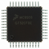
Manufacturer Part Number
MC9S08GT32CFDE
Description
IC MCU 32K FLASH 20MHZ 48-QFN
Manufacturer
Freescale Semiconductor
Series
HCS08r
Specifications of MC9S08GT32CFDE
Core Processor
HCS08
Core Size
8-Bit
Speed
40MHz
Connectivity
I²C, SCI, SPI
Peripherals
LVD, POR, PWM, WDT
Number Of I /o
39
Program Memory Size
32KB (32K x 8)
Program Memory Type
FLASH
Ram Size
2K x 8
Voltage - Supply (vcc/vdd)
1.8 V ~ 3.6 V
Data Converters
A/D 8x10b
Oscillator Type
Internal
Operating Temperature
-40°C ~ 85°C
Package / Case
48-QFN
Controller Family/series
HCS08
No. Of I/o's
39
Ram Memory Size
2KB
Cpu Speed
40MHz
No. Of Timers
2
Rohs Compliant
Yes
For Use With
M68DEMO908GB60E - BOARD DEMO MC9S08GB60M68EVB908GB60E - BOARD EVAL FOR MC9S08GB60
Lead Free Status / RoHS Status
Lead free / RoHS Compliant
Eeprom Size
-


Analog-to-Digital Converter (ATD) Module
conversion to the mode control unit. For V
to set the sampled signal level within itself without relying on the S/H machine to deliver them.
The mode control unit organizes the conversion, specifies the input sample channel, and moves the digital
output data from the SAR register to the result register. The result register consists of a dual-port register.
The SAR register writes data into the register through one port while the module data bus reads data out
of the register through the other port.
14.3.2
The S/H machine accepts analog signals and stores them as capacitor charge on a storage node located in
the SAR machine. Only one sample can be held at a time so the S/H machine and the SAR machine can
not run concurrently even though they are independent machines.
various resistors and capacitors.
When the S/H machine is not sampling, it disables its own internal clocks.The input analog signals are
unipolar. The signals must fall within the potential range of V
required to perform special conversions (i.e., convert V
Proper sampling is dependent on the following factors:
224
•
•
•
Analog source impedance (the real portion, R
— This is the resistive (or real, in the case of high frequencies) portion of the network driving the
analog input voltage V
Analog source capacitance (C
large enough) may help the analog source network charge the ATD input in the case of high R
ATD input resistance (R
circuit in the path between the external ATD input and the ATD sample and hold circuit. This
resistance varies with temperature, voltage, and process variation but a worst case number is
necessary to compute worst case sample error.
Sample and Hold
V
AIN
+
–
Figure 14-3. Resistor and Capacitor Placement
AIN
AIN
R
AS
.
C
– maximum value 7 kΩ) — This is the internal resistance of the ATD
AS
MC9S08GB/GT Data Sheet, Rev. 2.3
AS
) — This is the filtering capacitance on the analog input, which (if
REFL
INPUT PIN
INPUT PIN
INPUT PIN
INPUT PIN
and V
R
R
R
R
REFH
AIN1
AIN2
AIN3
AINn
AS
.
.
.
REFL
– see
CHANNEL
SELECT 0
CHANNEL
SELECT 1
CHANNEL
SELECT 2
CHANNEL
SELECT n
, the SAR machine uses the reference potentials
and V
SSAD
Appendix A, “Electrical
Figure 14-3
C
REFH
to V
AIN
).
DDAD
ATD SAR
ENGINE
shows the placement of the
. The S/H machine is not
Freescale Semiconductor
Characteristics”)
AS
.
Related parts for MC9S08GT32CFDE
Image
Part Number
Description
Manufacturer
Datasheet
Request
R

Part Number:
Description:
Manufacturer:
Freescale Semiconductor, Inc
Datasheet:
Part Number:
Description:
Manufacturer:
Freescale Semiconductor, Inc
Datasheet:
Part Number:
Description:
Manufacturer:
Freescale Semiconductor, Inc
Datasheet:
Part Number:
Description:
Manufacturer:
Freescale Semiconductor, Inc
Datasheet:
Part Number:
Description:
Manufacturer:
Freescale Semiconductor, Inc
Datasheet:
Part Number:
Description:
Manufacturer:
Freescale Semiconductor, Inc
Datasheet:
Part Number:
Description:
Manufacturer:
Freescale Semiconductor, Inc
Datasheet:
Part Number:
Description:
Manufacturer:
Freescale Semiconductor, Inc
Datasheet:
Part Number:
Description:
Manufacturer:
Freescale Semiconductor, Inc
Datasheet:
Part Number:
Description:
Manufacturer:
Freescale Semiconductor, Inc
Datasheet:
Part Number:
Description:
Manufacturer:
Freescale Semiconductor, Inc
Datasheet:
Part Number:
Description:
Manufacturer:
Freescale Semiconductor, Inc
Datasheet:
Part Number:
Description:
Manufacturer:
Freescale Semiconductor, Inc
Datasheet:
Part Number:
Description:
Manufacturer:
Freescale Semiconductor, Inc
Datasheet:
Part Number:
Description:
Manufacturer:
Freescale Semiconductor, Inc
Datasheet: