MC9S08GT32CFDE Freescale Semiconductor, MC9S08GT32CFDE Datasheet - Page 154
MC9S08GT32CFDE
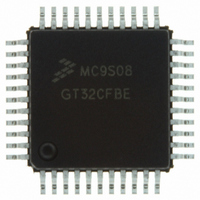
Manufacturer Part Number
MC9S08GT32CFDE
Description
IC MCU 32K FLASH 20MHZ 48-QFN
Manufacturer
Freescale Semiconductor
Series
HCS08r
Specifications of MC9S08GT32CFDE
Core Processor
HCS08
Core Size
8-Bit
Speed
40MHz
Connectivity
I²C, SCI, SPI
Peripherals
LVD, POR, PWM, WDT
Number Of I /o
39
Program Memory Size
32KB (32K x 8)
Program Memory Type
FLASH
Ram Size
2K x 8
Voltage - Supply (vcc/vdd)
1.8 V ~ 3.6 V
Data Converters
A/D 8x10b
Oscillator Type
Internal
Operating Temperature
-40°C ~ 85°C
Package / Case
48-QFN
Controller Family/series
HCS08
No. Of I/o's
39
Ram Memory Size
2KB
Cpu Speed
40MHz
No. Of Timers
2
Rohs Compliant
Yes
For Use With
M68DEMO908GB60E - BOARD DEMO MC9S08GB60M68EVB908GB60E - BOARD EVAL FOR MC9S08GB60
Lead Free Status / RoHS Status
Lead free / RoHS Compliant
Eeprom Size
-


Timer/PWM (TPM) Module
counter (when operating in normal up-counting mode) provides the timing reference for the input capture,
output compare, and edge-aligned PWM functions. The timer counter modulo registers,
TPMxMODH:TPMxMODL, control the modulo value of the counter. (The values $0000 or $FFFF
effectively make the counter free running.) Software can read the counter value at any time without
affecting the counting sequence. Any write to either byte of the TPMxCNT counter resets the counter
regardless of the data value written.
All TPM channels are programmable independently as input capture, output compare, or buffered
edge-aligned PWM channels.
10.4
Table 10-1
clock input, the associated TPM channel 0 can not use the pin. (Channel 0 can still be used in output
compare mode as a software timer.) When any of the pins associated with the timer is configured as a timer
input, a passive pullup can be enabled. After reset, the TPM modules are disabled and all pins default to
general-purpose inputs with the passive pullups disabled.
10.4.1
When control bits CLKSB:CLKSA in the timer status and control register are set to 1:1, the prescaler and
consequently the 16-bit counter for TPMx are driven by an external clock source connected to the
TPMxCH0 pin. A synchronizer is needed between the external clock and the rest of the TPM. This
synchronizer is clocked by the bus clock so the frequency of the external source must be less than one-half
the frequency of the bus rate clock. The upper frequency limit for this external clock source is specified to
be one-fourth the bus frequency to conservatively accommodate duty cycle and phase-locked loop (PLL)
or frequency-locked loop (FLL) frequency jitter effects.
When the TPM is using the channel 0 pin for an external clock, the corresponding ELS0B:ELS0A control
bits should be set to 0:0 so channel 0 is not trying to use the same pin.
10.4.2
Each TPM channel is associated with an I/O pin on the MCU. The function of this pin depends on the
configuration of the channel. In some cases, no pin function is needed so the pin reverts to being controlled
by general-purpose I/O controls. When a timer has control of a port pin, the port data and data direction
registers do not affect the related pin(s). See the
about shared pin functions.
10.5
All TPM functions are associated with a main 16-bit counter that allows flexible selection of the clock
source and prescale divisor. A 16-bit modulo register also is associated with the main 16-bit counter in the
TPM. Each TPM channel is optionally associated with an MCU pin and a maskable interrupt function.
The TPM has center-aligned PWM capabilities controlled by the CPWMS control bit in TPMxSC. When
CPWMS is set to 1, timer counter TPMxCNT changes to an up-/down-counter and all channels in the
154
Pin Descriptions
Functional Description
shows the MCU pins related to the TPM modules. When TPMxCH0 is used as an external
External TPM Clock Sources
TPMxCHn — TPMx Channel n I/O Pins
MC9S08GB/GT Data Sheet, Rev. 2.3
Pins and Connections
chapter for additional information
Freescale Semiconductor
Related parts for MC9S08GT32CFDE
Image
Part Number
Description
Manufacturer
Datasheet
Request
R

Part Number:
Description:
Manufacturer:
Freescale Semiconductor, Inc
Datasheet:
Part Number:
Description:
Manufacturer:
Freescale Semiconductor, Inc
Datasheet:
Part Number:
Description:
Manufacturer:
Freescale Semiconductor, Inc
Datasheet:
Part Number:
Description:
Manufacturer:
Freescale Semiconductor, Inc
Datasheet:
Part Number:
Description:
Manufacturer:
Freescale Semiconductor, Inc
Datasheet:
Part Number:
Description:
Manufacturer:
Freescale Semiconductor, Inc
Datasheet:
Part Number:
Description:
Manufacturer:
Freescale Semiconductor, Inc
Datasheet:
Part Number:
Description:
Manufacturer:
Freescale Semiconductor, Inc
Datasheet:
Part Number:
Description:
Manufacturer:
Freescale Semiconductor, Inc
Datasheet:
Part Number:
Description:
Manufacturer:
Freescale Semiconductor, Inc
Datasheet:
Part Number:
Description:
Manufacturer:
Freescale Semiconductor, Inc
Datasheet:
Part Number:
Description:
Manufacturer:
Freescale Semiconductor, Inc
Datasheet:
Part Number:
Description:
Manufacturer:
Freescale Semiconductor, Inc
Datasheet:
Part Number:
Description:
Manufacturer:
Freescale Semiconductor, Inc
Datasheet:
Part Number:
Description:
Manufacturer:
Freescale Semiconductor, Inc
Datasheet: