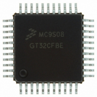
MC9S08GT32CFDE Freescale Semiconductor, MC9S08GT32CFDE Datasheet - Page 171

MC9S08GT32CFDE
Manufacturer Part Number
MC9S08GT32CFDE
Description
IC MCU 32K FLASH 20MHZ 48-QFN
Manufacturer
Freescale Semiconductor
Series
HCS08r
Specifications of MC9S08GT32CFDE
Core Processor
HCS08
Core Size
8-Bit
Speed
40MHz
Connectivity
I²C, SCI, SPI
Peripherals
LVD, POR, PWM, WDT
Number Of I /o
39
Program Memory Size
32KB (32K x 8)
Program Memory Type
FLASH
Ram Size
2K x 8
Voltage - Supply (vcc/vdd)
1.8 V ~ 3.6 V
Data Converters
A/D 8x10b
Oscillator Type
Internal
Operating Temperature
-40°C ~ 85°C
Package / Case
48-QFN
Controller Family/series
HCS08
No. Of I/o's
39
Ram Memory Size
2KB
Cpu Speed
40MHz
No. Of Timers
2
Rohs Compliant
Yes
For Use With
M68DEMO908GB60E - BOARD DEMO MC9S08GB60M68EVB908GB60E - BOARD EVAL FOR MC9S08GB60
Lead Free Status / RoHS Status
Lead free / RoHS Compliant
Eeprom Size
-
- Current page: 171 of 290
- Download datasheet (2Mb)
The transmitter is enabled by setting the TE bit in SCIxC2. This queues a preamble character that is one
full character frame of logic high. The transmitter then remains idle (TxD1 pin remains high) until data is
available in the transmit data buffer. Programs store data into the transmit data buffer by writing to the SCI
data register (SCIxD).
The central element of the SCI transmitter is the transmit shift register that is either 10 or 11 bits long
depending on the setting in the M control bit. For the remainder of this section, we will assume M = 0,
selecting the normal 8-bit data mode. In 8-bit data mode, the shift register holds a start bit, eight data bits,
and a stop bit. When the transmit shift register is available for a new SCI character, the value waiting in
the transmit data register is transferred to the shift register (synchronized with the baud rate clock) and the
transmit data register empty (TDRE) status flag is set to indicate another character may be written to the
transmit data buffer at SCIxD.
Freescale Semiconductor
RATE CLOCK
1 × BAUD
INTERNAL BUS
PE
TE
PT
M
ENABLE
TXDIR
SBK
Figure 11-3. SCI Transmitter Block Diagram
GENERATION
PARITY
T8
MC9S08GB/GT Data Sheet, Rev. 2.3
H
(WRITE-ONLY)
8
11-BIT TRANSMIT SHIFT REGISTER
7
6
SCID – Tx BUFFER
TRANSMIT CONTROL
SHIFT DIRECTION
5
4
TDRE
TCIE
TIE
TC
3
2
1
0
L
LOOPS
SCI CONTROLS TxD1
TxD1 DIRECTION
RSRC
CONTROL
Transmitter Functional Description
LOOP
Tx INTERRUPT
REQUEST
TO RECEIVE
DATA IN
TO TxD1 PIN
TO TxD1
PIN LOGIC
171
Related parts for MC9S08GT32CFDE
Image
Part Number
Description
Manufacturer
Datasheet
Request
R
Part Number:
Description:
Manufacturer:
Freescale Semiconductor, Inc
Datasheet:
Part Number:
Description:
Manufacturer:
Freescale Semiconductor, Inc
Datasheet:
Part Number:
Description:
Manufacturer:
Freescale Semiconductor, Inc
Datasheet:
Part Number:
Description:
Manufacturer:
Freescale Semiconductor, Inc
Datasheet:
Part Number:
Description:
Manufacturer:
Freescale Semiconductor, Inc
Datasheet:
Part Number:
Description:
Manufacturer:
Freescale Semiconductor, Inc
Datasheet:
Part Number:
Description:
Manufacturer:
Freescale Semiconductor, Inc
Datasheet:
Part Number:
Description:
Manufacturer:
Freescale Semiconductor, Inc
Datasheet:
Part Number:
Description:
Manufacturer:
Freescale Semiconductor, Inc
Datasheet:
Part Number:
Description:
Manufacturer:
Freescale Semiconductor, Inc
Datasheet:
Part Number:
Description:
Manufacturer:
Freescale Semiconductor, Inc
Datasheet:
Part Number:
Description:
Manufacturer:
Freescale Semiconductor, Inc
Datasheet:
Part Number:
Description:
Manufacturer:
Freescale Semiconductor, Inc
Datasheet:
Part Number:
Description:
Manufacturer:
Freescale Semiconductor, Inc
Datasheet:
Part Number:
Description:
Manufacturer:
Freescale Semiconductor, Inc
Datasheet:


