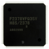
DF2378BVFQ35V Renesas Electronics America, DF2378BVFQ35V Datasheet - Page 18
DF2378BVFQ35V
Manufacturer Part Number
DF2378BVFQ35V
Description
IC H8S/2378 MCU FLASH 144-LQFP
Manufacturer
Renesas Electronics America
Series
H8® H8S/2300r
Specifications of DF2378BVFQ35V
Core Processor
H8S/2000
Core Size
16-Bit
Speed
35MHz
Connectivity
I²C, IrDA, SCI, SmartCard
Peripherals
DMA, POR, PWM, WDT
Number Of I /o
97
Program Memory Size
512KB (512K x 8)
Program Memory Type
FLASH
Ram Size
32K x 8
Voltage - Supply (vcc/vdd)
3 V ~ 3.6 V
Data Converters
A/D 16x10b; D/A 6x8b
Oscillator Type
Internal
Operating Temperature
-20°C ~ 75°C
Package / Case
144-LQFP
For Use With
YLCDRSK2378 - KIT DEV EVAL H8S/2378 LCDYR0K42378FC000BA - KIT EVAL FOR H8S/2378HS0005KCU11H - EMULATOR E10A-USB H8S(X),SH2(A)EDK2378 - DEV EVAL KIT FOR H8S/2378
Lead Free Status / RoHS Status
Lead free / RoHS Compliant
Eeprom Size
-
Available stocks
Company
Part Number
Manufacturer
Quantity
Price
Company:

Part Number:
DF2378BVFQ35V
Manufacturer:
Renesas Electronics America
Quantity:
135
Company:
Part Number:
DF2378BVFQ35V
Manufacturer:
Renesas Electronics America
Quantity:
10 000


Item
17.1 Features
Figure 17.1 Block
Diagram of A/D
Converter
21.1 Features
21.1.1 Operating
Mode
21.3.1 Programming/
Erasing Interface
Register
21.3.2 Programming/
Erasing Interface
Parameter
21.3.3 Flash Vector
Address Control
Register (FVACR)
Rev.7.00 Mar. 18, 2009 page xvi of lxvi
REJ09B0109-0700
Page
806
862
864
872
879
889
Revision (See Manual for Details)
Figure amended
Description amended
• Programming/erase protection
Description amended
When the mode pins are set in the reset state and a reset start
is performed, the MCU transitions to an operating mode as
shown in figure 21.2.
Description amended
• Flash Code Control and Status Register (FCCS)
Description amended
When download, initialization, or on-chip program is executed,
registers of the CPU except for ER0 and ER1 are stored. The
return value of the processing result is written in ER0, ER1.
Since the stack area is used for storing the registers except for
ER0, ER1, the stack area must be saved at the processing start.
(A maximum size of a stack area to be used is 128 bytes.)
Description amended
FVACR modifies the space from which the vector table data of
the NMI interrupts is read. Normally the vector table data is read
from the address spaces from H'00001C to H'00001F.
There are three types of flash memory programming/erase
FCCS is used to request monitoring of flash memory
protection that may be selected: hardware protection,
software protection, and error protection.
programming/erase errors or downloading of on-chip
programs.
AVCC
Vref
AVSS
10-bit D/A
Related parts for DF2378BVFQ35V
Image
Part Number
Description
Manufacturer
Datasheet
Request
R

Part Number:
Description:
KIT STARTER FOR M16C/29
Manufacturer:
Renesas Electronics America
Datasheet:

Part Number:
Description:
KIT STARTER FOR R8C/2D
Manufacturer:
Renesas Electronics America
Datasheet:

Part Number:
Description:
R0K33062P STARTER KIT
Manufacturer:
Renesas Electronics America
Datasheet:

Part Number:
Description:
KIT STARTER FOR R8C/23 E8A
Manufacturer:
Renesas Electronics America
Datasheet:

Part Number:
Description:
KIT STARTER FOR R8C/25
Manufacturer:
Renesas Electronics America
Datasheet:

Part Number:
Description:
KIT STARTER H8S2456 SHARPE DSPLY
Manufacturer:
Renesas Electronics America
Datasheet:

Part Number:
Description:
KIT STARTER FOR R8C38C
Manufacturer:
Renesas Electronics America
Datasheet:

Part Number:
Description:
KIT STARTER FOR R8C35C
Manufacturer:
Renesas Electronics America
Datasheet:

Part Number:
Description:
KIT STARTER FOR R8CL3AC+LCD APPS
Manufacturer:
Renesas Electronics America
Datasheet:
Part Number:
Description:
KIT STARTER FOR RX610
Manufacturer:
Renesas Electronics America
Datasheet:

Part Number:
Description:
KIT STARTER FOR R32C/118
Manufacturer:
Renesas Electronics America
Datasheet:

Part Number:
Description:
KIT DEV RSK-R8C/26-29
Manufacturer:
Renesas Electronics America
Datasheet:

Part Number:
Description:
KIT STARTER FOR SH7124
Manufacturer:
Renesas Electronics America
Datasheet:

Part Number:
Description:
KIT STARTER FOR H8SX/1622
Manufacturer:
Renesas Electronics America
Datasheet:

Part Number:
Description:
KIT DEV FOR SH7203
Manufacturer:
Renesas Electronics America
Datasheet: