DF2378BVFQ35V Renesas Electronics America, DF2378BVFQ35V Datasheet - Page 927
DF2378BVFQ35V
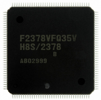
Manufacturer Part Number
DF2378BVFQ35V
Description
IC H8S/2378 MCU FLASH 144-LQFP
Manufacturer
Renesas Electronics America
Series
H8® H8S/2300r
Specifications of DF2378BVFQ35V
Core Processor
H8S/2000
Core Size
16-Bit
Speed
35MHz
Connectivity
I²C, IrDA, SCI, SmartCard
Peripherals
DMA, POR, PWM, WDT
Number Of I /o
97
Program Memory Size
512KB (512K x 8)
Program Memory Type
FLASH
Ram Size
32K x 8
Voltage - Supply (vcc/vdd)
3 V ~ 3.6 V
Data Converters
A/D 16x10b; D/A 6x8b
Oscillator Type
Internal
Operating Temperature
-20°C ~ 75°C
Package / Case
144-LQFP
For Use With
YLCDRSK2378 - KIT DEV EVAL H8S/2378 LCDYR0K42378FC000BA - KIT EVAL FOR H8S/2378HS0005KCU11H - EMULATOR E10A-USB H8S(X),SH2(A)EDK2378 - DEV EVAL KIT FOR H8S/2378
Lead Free Status / RoHS Status
Lead free / RoHS Compliant
Eeprom Size
-
Available stocks
Company
Part Number
Manufacturer
Quantity
Price
Company:

Part Number:
DF2378BVFQ35V
Manufacturer:
Renesas Electronics America
Quantity:
135
Company:
Part Number:
DF2378BVFQ35V
Manufacturer:
Renesas Electronics America
Quantity:
10 000


φ
V
MD2 to MD0
RES
SWE bit
CC
Notes: 1. When entering boot mode or making a transition from boot mode to another mode, mode switching must be
Period during which flash memory access is prohibited
(x: Wait time after setting SWE bit)*
Period during which flash memory can be programmed
(Execution of program in flash memory prohibited, and data reads other than verify operations prohibited)
2. When making a transition from boot mode to another mode, a mode programming setup time t
3. See section 26.1.6, Flash Memory Characteristics.
4. Wait time: 100 μs
carried out by means of RES input. The state of ports with multiplexed address functions and bus control output
pins (AS, RD, HWR, LWR) will change during this switchover interval (the interval during which the RES pin
input is low), and therefore these pins should not be used as output signals during this time.
ns is necessary with respect to RES clearance timing.
t
(Example: Boot Mode → User Mode ↔ User Program Mode)
OSC1
Mode
change
t
SWE
set
MDS
*
1
Wait time: x
Programming/erasing
possible
Figure 20.10 Mode Transition Timing
Boot
mode
3
*
4
SWE
cleared
Mode
change
t
RESW
t
MDS
*
*
1
Section 20 Flash Memory (0.35-μm F-ZTAT Version)
2
Wait time: x
Programming/erasing
possible
User
mode
User
program
mode
Rev.7.00 Mar. 18, 2009 page 859 of 1136
*
User
mode
4
Wait time: x
Programming/erasing
possible
User
program
mode
*
4
User mode
REJ09B0109-0700
MDS
Wait time: x
Programming/erasing
possible
User
program
mode
(min.) of 200
*
4
Related parts for DF2378BVFQ35V
Image
Part Number
Description
Manufacturer
Datasheet
Request
R

Part Number:
Description:
KIT STARTER FOR M16C/29
Manufacturer:
Renesas Electronics America
Datasheet:

Part Number:
Description:
KIT STARTER FOR R8C/2D
Manufacturer:
Renesas Electronics America
Datasheet:

Part Number:
Description:
R0K33062P STARTER KIT
Manufacturer:
Renesas Electronics America
Datasheet:

Part Number:
Description:
KIT STARTER FOR R8C/23 E8A
Manufacturer:
Renesas Electronics America
Datasheet:

Part Number:
Description:
KIT STARTER FOR R8C/25
Manufacturer:
Renesas Electronics America
Datasheet:

Part Number:
Description:
KIT STARTER H8S2456 SHARPE DSPLY
Manufacturer:
Renesas Electronics America
Datasheet:

Part Number:
Description:
KIT STARTER FOR R8C38C
Manufacturer:
Renesas Electronics America
Datasheet:

Part Number:
Description:
KIT STARTER FOR R8C35C
Manufacturer:
Renesas Electronics America
Datasheet:

Part Number:
Description:
KIT STARTER FOR R8CL3AC+LCD APPS
Manufacturer:
Renesas Electronics America
Datasheet:
Part Number:
Description:
KIT STARTER FOR RX610
Manufacturer:
Renesas Electronics America
Datasheet:

Part Number:
Description:
KIT STARTER FOR R32C/118
Manufacturer:
Renesas Electronics America
Datasheet:

Part Number:
Description:
KIT DEV RSK-R8C/26-29
Manufacturer:
Renesas Electronics America
Datasheet:

Part Number:
Description:
KIT STARTER FOR SH7124
Manufacturer:
Renesas Electronics America
Datasheet:

Part Number:
Description:
KIT STARTER FOR H8SX/1622
Manufacturer:
Renesas Electronics America
Datasheet:

Part Number:
Description:
KIT DEV FOR SH7203
Manufacturer:
Renesas Electronics America
Datasheet: