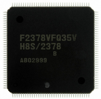
DF2378BVFQ35V Renesas Electronics America, DF2378BVFQ35V Datasheet - Page 992

DF2378BVFQ35V
Manufacturer Part Number
DF2378BVFQ35V
Description
IC H8S/2378 MCU FLASH 144-LQFP
Manufacturer
Renesas Electronics America
Series
H8® H8S/2300r
Specifications of DF2378BVFQ35V
Core Processor
H8S/2000
Core Size
16-Bit
Speed
35MHz
Connectivity
I²C, IrDA, SCI, SmartCard
Peripherals
DMA, POR, PWM, WDT
Number Of I /o
97
Program Memory Size
512KB (512K x 8)
Program Memory Type
FLASH
Ram Size
32K x 8
Voltage - Supply (vcc/vdd)
3 V ~ 3.6 V
Data Converters
A/D 16x10b; D/A 6x8b
Oscillator Type
Internal
Operating Temperature
-20°C ~ 75°C
Package / Case
144-LQFP
For Use With
YLCDRSK2378 - KIT DEV EVAL H8S/2378 LCDYR0K42378FC000BA - KIT EVAL FOR H8S/2378HS0005KCU11H - EMULATOR E10A-USB H8S(X),SH2(A)EDK2378 - DEV EVAL KIT FOR H8S/2378
Lead Free Status / RoHS Status
Lead free / RoHS Compliant
Eeprom Size
-
Available stocks
Company
Part Number
Manufacturer
Quantity
Price
Company:
Part Number:
DF2378BVFQ35V
Manufacturer:
Renesas Electronics America
Quantity:
135
Company:
Part Number:
DF2378BVFQ35V
Manufacturer:
Renesas Electronics America
Quantity:
10 000
- Current page: 992 of 1208
- Download datasheet (8Mb)
Section 21 Flash Memory (0.18-μm F-ZTAT Version)
21.7
Along with its on-board programming mode, this LSI also has a PROM mode as a further mode
for the writing and erasing of programs and data. In the PROM mode, a general-purpose PROM
programmer can freely be used to write programs to the on-chip ROM. Program/erase is possible
on the user MAT and user boot MAT. The PROM programmer must support Renesas
microcomputers with 512-kbyte flash memory as a device type.
A status-polling system is adopted for operation in automatic program, automatic erase, and
status-read modes. In the status-read mode, details of the system’s internal signals are output after
execution of automatic programming or automatic erasure. In the PROM mode, provide a 12-MHz
input-clock signal.
21.8
Initiating boot mode enables the boot program to communicate with the host by using the internal
SCI. The serial communication interface specification is shown below.
(1)
The boot program has three states.
1. Bit-Rate-Adjustment State
2. Inquiry/Selection State
3. Programming/erasing state
These boot program states are shown in figure 21.17.
Rev.7.00 Mar. 18, 2009 page 924 of 1136
REJ09B0109-0700
In this state, the boot program adjusts the bit rate to communicate with the host. Initiating boot
mode enables starting of the boot program and entry to the bit-rate-adjustment state. The
program receives the command from the host to adjust the bit rate. After adjusting the bit rate,
the program enters the inquiry/selection state.
In this state, the boot program responds to inquiry commands from the host. The device name,
clock mode, and bit rate are selected. After selection of these settings, the program is made to
enter the programming/erasing state by the command for a transition to the
programming/erasing state. The program transfers the libraries required for erasure to the
RAM and erases the user MATs and user boot MATs before the transition.
Programming and erasure by the boot program take place in this state. The boot program is
made to transfer the programming/erasing programs to the RAM by commands from the host.
Sum checks and blank checks are executed by sending these commands from the host.
Status
Programmer Mode
Serial Communication Interface Specification for Boot Mode
Related parts for DF2378BVFQ35V
Image
Part Number
Description
Manufacturer
Datasheet
Request
R

Part Number:
Description:
KIT STARTER FOR M16C/29
Manufacturer:
Renesas Electronics America
Datasheet:

Part Number:
Description:
KIT STARTER FOR R8C/2D
Manufacturer:
Renesas Electronics America
Datasheet:

Part Number:
Description:
R0K33062P STARTER KIT
Manufacturer:
Renesas Electronics America
Datasheet:

Part Number:
Description:
KIT STARTER FOR R8C/23 E8A
Manufacturer:
Renesas Electronics America
Datasheet:

Part Number:
Description:
KIT STARTER FOR R8C/25
Manufacturer:
Renesas Electronics America
Datasheet:

Part Number:
Description:
KIT STARTER H8S2456 SHARPE DSPLY
Manufacturer:
Renesas Electronics America
Datasheet:

Part Number:
Description:
KIT STARTER FOR R8C38C
Manufacturer:
Renesas Electronics America
Datasheet:

Part Number:
Description:
KIT STARTER FOR R8C35C
Manufacturer:
Renesas Electronics America
Datasheet:

Part Number:
Description:
KIT STARTER FOR R8CL3AC+LCD APPS
Manufacturer:
Renesas Electronics America
Datasheet:

Part Number:
Description:
KIT STARTER FOR RX610
Manufacturer:
Renesas Electronics America
Datasheet:

Part Number:
Description:
KIT STARTER FOR R32C/118
Manufacturer:
Renesas Electronics America
Datasheet:

Part Number:
Description:
KIT DEV RSK-R8C/26-29
Manufacturer:
Renesas Electronics America
Datasheet:

Part Number:
Description:
KIT STARTER FOR SH7124
Manufacturer:
Renesas Electronics America
Datasheet:

Part Number:
Description:
KIT STARTER FOR H8SX/1622
Manufacturer:
Renesas Electronics America
Datasheet:

Part Number:
Description:
KIT DEV FOR SH7203
Manufacturer:
Renesas Electronics America
Datasheet:


