DF2378BVFQ35V Renesas Electronics America, DF2378BVFQ35V Datasheet - Page 424
DF2378BVFQ35V
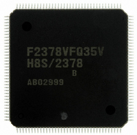
Manufacturer Part Number
DF2378BVFQ35V
Description
IC H8S/2378 MCU FLASH 144-LQFP
Manufacturer
Renesas Electronics America
Series
H8® H8S/2300r
Specifications of DF2378BVFQ35V
Core Processor
H8S/2000
Core Size
16-Bit
Speed
35MHz
Connectivity
I²C, IrDA, SCI, SmartCard
Peripherals
DMA, POR, PWM, WDT
Number Of I /o
97
Program Memory Size
512KB (512K x 8)
Program Memory Type
FLASH
Ram Size
32K x 8
Voltage - Supply (vcc/vdd)
3 V ~ 3.6 V
Data Converters
A/D 16x10b; D/A 6x8b
Oscillator Type
Internal
Operating Temperature
-20°C ~ 75°C
Package / Case
144-LQFP
For Use With
YLCDRSK2378 - KIT DEV EVAL H8S/2378 LCDYR0K42378FC000BA - KIT EVAL FOR H8S/2378HS0005KCU11H - EMULATOR E10A-USB H8S(X),SH2(A)EDK2378 - DEV EVAL KIT FOR H8S/2378
Lead Free Status / RoHS Status
Lead free / RoHS Compliant
Eeprom Size
-
Available stocks
Company
Part Number
Manufacturer
Quantity
Price
Company:

Part Number:
DF2378BVFQ35V
Manufacturer:
Renesas Electronics America
Quantity:
135
Company:
Part Number:
DF2378BVFQ35V
Manufacturer:
Renesas Electronics America
Quantity:
10 000


Section 7 DMA Controller (DMAC)
7.7.3
When the WDBE bit of BCR in the bus controller is set to 1, enabling the write data buffer
function, dual address transfer external write cycles or single address transfers and internal
accesses (on-chip memory or internal I/O registers) are executed in parallel.
• Write data buffer function and DMAC register setting
• Write data buffer function and DMAC operation timing
7.7.4
If the last transfer cycle is for an internal address, note that even if low-level output at the TEND
pin has been set, a low level may not be output at the TEND pin under the following external bus
conditions since the last transfer cycle (internal bus cycle) and the external bus cycle are executed
in parallel.
1. EXDMAC cycle
2. Write cycle with write buffer mode enabled
3. DMAC single address cycle for a different channel with write buffer mode enabled
4. Bus release cycle
5. CBR refresh cycle
Figure 7.41 shows an example in which a low level is not output from the TEND pin in case 2
above.
If the last transfer cycle is an external address cycle, a low level is output at the TEND pin in
synchronization with the bus cycle.
Rev.7.00 Mar. 18, 2009 page 356 of 1136
REJ09B0109-0700
If the setting of a register that controls external accesses is changed during execution of an
external access by means of the write data buffer function, the external access may not be
performed normally. Registers that control external accesses should only be manipulated when
external reads, etc., are used with DMAC operation disabled, and the operation is not
performed in parallel with external access.
The DMAC can start its next operation during external access using the write data buffer
function. Consequently, the DREQ pin sampling timing, TEND output timing, etc., are
different from the case in which the write data buffer function is disabled. Also, internal bus
cycles maybe hidden, and not visible.
Write Data Buffer Function
TEND Output
Related parts for DF2378BVFQ35V
Image
Part Number
Description
Manufacturer
Datasheet
Request
R

Part Number:
Description:
KIT STARTER FOR M16C/29
Manufacturer:
Renesas Electronics America
Datasheet:

Part Number:
Description:
KIT STARTER FOR R8C/2D
Manufacturer:
Renesas Electronics America
Datasheet:

Part Number:
Description:
R0K33062P STARTER KIT
Manufacturer:
Renesas Electronics America
Datasheet:

Part Number:
Description:
KIT STARTER FOR R8C/23 E8A
Manufacturer:
Renesas Electronics America
Datasheet:

Part Number:
Description:
KIT STARTER FOR R8C/25
Manufacturer:
Renesas Electronics America
Datasheet:

Part Number:
Description:
KIT STARTER H8S2456 SHARPE DSPLY
Manufacturer:
Renesas Electronics America
Datasheet:

Part Number:
Description:
KIT STARTER FOR R8C38C
Manufacturer:
Renesas Electronics America
Datasheet:

Part Number:
Description:
KIT STARTER FOR R8C35C
Manufacturer:
Renesas Electronics America
Datasheet:

Part Number:
Description:
KIT STARTER FOR R8CL3AC+LCD APPS
Manufacturer:
Renesas Electronics America
Datasheet:
Part Number:
Description:
KIT STARTER FOR RX610
Manufacturer:
Renesas Electronics America
Datasheet:

Part Number:
Description:
KIT STARTER FOR R32C/118
Manufacturer:
Renesas Electronics America
Datasheet:

Part Number:
Description:
KIT DEV RSK-R8C/26-29
Manufacturer:
Renesas Electronics America
Datasheet:

Part Number:
Description:
KIT STARTER FOR SH7124
Manufacturer:
Renesas Electronics America
Datasheet:

Part Number:
Description:
KIT STARTER FOR H8SX/1622
Manufacturer:
Renesas Electronics America
Datasheet:

Part Number:
Description:
KIT DEV FOR SH7203
Manufacturer:
Renesas Electronics America
Datasheet: