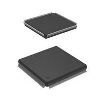
HD6417750RF200DV Renesas Electronics America, HD6417750RF200DV Datasheet - Page 330

HD6417750RF200DV
Manufacturer Part Number
HD6417750RF200DV
Description
MPU 1.5/3.3V 0K I-TEMP PB-FREE 2
Manufacturer
Renesas Electronics America
Series
SuperH® SH7750r
Datasheet
1.D6417750RBP240DV.pdf
(1164 pages)
Specifications of HD6417750RF200DV
Core Processor
SH-4
Core Size
32-Bit
Speed
200MHz
Connectivity
EBI/EMI, FIFO, SCI, SmartCard
Peripherals
DMA, POR, WDT
Number Of I /o
28
Program Memory Type
ROMless
Ram Size
48K x 8
Voltage - Supply (vcc/vdd)
1.35 V ~ 1.6 V
Oscillator Type
External
Operating Temperature
-40°C ~ 85°C
Package / Case
208-QFP Exposed Pad, 208-eQFP, 208-HQFP
Lead Free Status / RoHS Status
Lead free / RoHS Compliant
Eeprom Size
-
Program Memory Size
-
Data Converters
-
Available stocks
Company
Part Number
Manufacturer
Quantity
Price
Company:
Part Number:
HD6417750RF200DV
Manufacturer:
FREESCALE
Quantity:
450
- Current page: 330 of 1164
- Download datasheet (7Mb)
Section 8 Pipelining
operation, never occurs. For example, when FADD follows FDIV with no dependency between FP
registers, FADD is not stalled even if both instructions update the cause field of FPSCR.
Anti-flow dependency can occur only between a preceding double-precision FADD, FMUL,
FSUB, or FTRV and a following FMOV, FLDI0, FLDI1, FABS, FNEG, or FSTS. See figure 8.3
(g).
If an executing instruction locks any resource—i.e. a function block that performs a basic
operation—a following instruction that happens to attempt to use the locked resource must be
stalled (figure 8.3 (h)). This kind of stall can be compensated by inserting one or more instructions
independent of the locked resource to separate the interfering instructions. For example, when a
load instruction and an ADD instruction that references the loaded value are consecutive, the 2-
cycle stall of the ADD is eliminated by inserting three instructions without dependency. Software
performance can be improved by such instruction scheduling.
Other penalties arise in the event of exceptions or external data accesses, as follows.
• Instruction TLB miss
• Instruction access to external memory (instruction cache miss, etc.)
• Data access to external memory (operand cache miss, etc.)
• Data access to a memory-mapped control register.
During the penalty cycles of an instruction TLB miss or external instruction access, no instruction
is issued, but execution of instructions that have already been issued continues. The penalty for a
data access is a pipeline freeze: that is, the execution of uncompleted instructions is interrupted
until the arrival of the requested data. The number of penalty cycles for instruction and data
accesses is largely dependent on the user's memory subsystems.
Rev.7.00 Oct. 10, 2008 Page 244 of 1074
REJ09B0366-0700
Related parts for HD6417750RF200DV
Image
Part Number
Description
Manufacturer
Datasheet
Request
R

Part Number:
Description:
KIT STARTER FOR M16C/29
Manufacturer:
Renesas Electronics America
Datasheet:

Part Number:
Description:
KIT STARTER FOR R8C/2D
Manufacturer:
Renesas Electronics America
Datasheet:

Part Number:
Description:
R0K33062P STARTER KIT
Manufacturer:
Renesas Electronics America
Datasheet:

Part Number:
Description:
KIT STARTER FOR R8C/23 E8A
Manufacturer:
Renesas Electronics America
Datasheet:

Part Number:
Description:
KIT STARTER FOR R8C/25
Manufacturer:
Renesas Electronics America
Datasheet:

Part Number:
Description:
KIT STARTER H8S2456 SHARPE DSPLY
Manufacturer:
Renesas Electronics America
Datasheet:

Part Number:
Description:
KIT STARTER FOR R8C38C
Manufacturer:
Renesas Electronics America
Datasheet:

Part Number:
Description:
KIT STARTER FOR R8C35C
Manufacturer:
Renesas Electronics America
Datasheet:

Part Number:
Description:
KIT STARTER FOR R8CL3AC+LCD APPS
Manufacturer:
Renesas Electronics America
Datasheet:

Part Number:
Description:
KIT STARTER FOR RX610
Manufacturer:
Renesas Electronics America
Datasheet:

Part Number:
Description:
KIT STARTER FOR R32C/118
Manufacturer:
Renesas Electronics America
Datasheet:

Part Number:
Description:
KIT DEV RSK-R8C/26-29
Manufacturer:
Renesas Electronics America
Datasheet:

Part Number:
Description:
KIT STARTER FOR SH7124
Manufacturer:
Renesas Electronics America
Datasheet:

Part Number:
Description:
KIT STARTER FOR H8SX/1622
Manufacturer:
Renesas Electronics America
Datasheet:

Part Number:
Description:
KIT DEV FOR SH7203
Manufacturer:
Renesas Electronics America
Datasheet:


