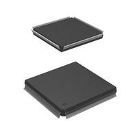
HD6417750RF200DV Renesas Electronics America, HD6417750RF200DV Datasheet - Page 951

HD6417750RF200DV
Manufacturer Part Number
HD6417750RF200DV
Description
MPU 1.5/3.3V 0K I-TEMP PB-FREE 2
Manufacturer
Renesas Electronics America
Series
SuperH® SH7750r
Datasheet
1.D6417750RBP240DV.pdf
(1164 pages)
Specifications of HD6417750RF200DV
Core Processor
SH-4
Core Size
32-Bit
Speed
200MHz
Connectivity
EBI/EMI, FIFO, SCI, SmartCard
Peripherals
DMA, POR, WDT
Number Of I /o
28
Program Memory Type
ROMless
Ram Size
48K x 8
Voltage - Supply (vcc/vdd)
1.35 V ~ 1.6 V
Oscillator Type
External
Operating Temperature
-40°C ~ 85°C
Package / Case
208-QFP Exposed Pad, 208-eQFP, 208-HQFP
Lead Free Status / RoHS Status
Lead free / RoHS Compliant
Eeprom Size
-
Program Memory Size
-
Data Converters
-
Available stocks
Company
Part Number
Manufacturer
Quantity
Price
Company:
Part Number:
HD6417750RF200DV
Manufacturer:
FREESCALE
Quantity:
450
- Current page: 951 of 1164
- Download datasheet (7Mb)
• Example of sequence of instructions with a branch (however, the example of a sequence of
20.3.3
The sequence of operations from setting of break conditions to user break exception handling is
described below.
1. Specify pre- or post-execution breaking in the case of an instruction access, inclusion or
2. Set the break bus conditions in the break bus cycle registers (BBRA, BBRB). If even one of
3. The operation when a break condition is satisfied depends on the BL bit (in the CPU's SR
instructions with no branch should be applied when the branch destination of a delayed branch
instruction is the instruction itself + 4):
L200 200 Instruction C (3 instructions after instruction A, 2 instructions after instruction B)
exclusion of the data bus value in the break conditions in the case of an operand access, and
use of independent or sequential channel A and B break conditions, in the break control
register (BRCR). Set the break addresses in the break address registers for each channel
(BARA, BARB), the ASIDs corresponding to the break space in the break ASID registers
(BASRA, BASRB), and the address and ASID masking methods in the break address mask
registers (BAMRA, BAMRB). If the data bus value is to be included in the break conditions,
also set the break data in the break data register (BDRB) and the data mask in the break data
mask register (BDMRB).
the BBRA/BBRB instruction access/operand access select (ID bit) and read/write select groups
(RW bit) is set to 00, a user break interrupt will not be generated on the corresponding channel.
Make the BBRA and BBRB settings after all other break-related register settings have been
completed. If breaks are enabled with BBRA/BBRB while the break address, data, or mask
register, or the break control register is in the initial state after a reset, a break may be
generated inadvertently.
register). When the BL bit is 0, exception handling is started and the condition match flag
(CMFA/CMFB) for the respective channel is set for the matched condition. When the BL bit is
1, the condition match flag (CMFA/CMFB) for the respective channel is set for the matched
condition but exception handling is not started.
The condition match flags (CMFA, CMFB) are set by a branch condition match, but are not
automatically cleared. Therefore, a memory store instruction should be used on the BRCR
User Break Operation Sequence
100 Instruction A: BT/S L200 (0 instructions after instruction A)
102 Instruction B (1 instruction after instruction A, 0 instructions after instruction B)
202 Instruction D (4 instructions after instruction A, 3 instructions after instruction B)
Rev.7.00 Oct. 10, 2008 Page 865 of 1074
Section 20 User Break Controller (UBC)
REJ09B0366-0700
Related parts for HD6417750RF200DV
Image
Part Number
Description
Manufacturer
Datasheet
Request
R

Part Number:
Description:
KIT STARTER FOR M16C/29
Manufacturer:
Renesas Electronics America
Datasheet:

Part Number:
Description:
KIT STARTER FOR R8C/2D
Manufacturer:
Renesas Electronics America
Datasheet:

Part Number:
Description:
R0K33062P STARTER KIT
Manufacturer:
Renesas Electronics America
Datasheet:

Part Number:
Description:
KIT STARTER FOR R8C/23 E8A
Manufacturer:
Renesas Electronics America
Datasheet:

Part Number:
Description:
KIT STARTER FOR R8C/25
Manufacturer:
Renesas Electronics America
Datasheet:

Part Number:
Description:
KIT STARTER H8S2456 SHARPE DSPLY
Manufacturer:
Renesas Electronics America
Datasheet:

Part Number:
Description:
KIT STARTER FOR R8C38C
Manufacturer:
Renesas Electronics America
Datasheet:

Part Number:
Description:
KIT STARTER FOR R8C35C
Manufacturer:
Renesas Electronics America
Datasheet:

Part Number:
Description:
KIT STARTER FOR R8CL3AC+LCD APPS
Manufacturer:
Renesas Electronics America
Datasheet:

Part Number:
Description:
KIT STARTER FOR RX610
Manufacturer:
Renesas Electronics America
Datasheet:

Part Number:
Description:
KIT STARTER FOR R32C/118
Manufacturer:
Renesas Electronics America
Datasheet:

Part Number:
Description:
KIT DEV RSK-R8C/26-29
Manufacturer:
Renesas Electronics America
Datasheet:

Part Number:
Description:
KIT STARTER FOR SH7124
Manufacturer:
Renesas Electronics America
Datasheet:

Part Number:
Description:
KIT STARTER FOR H8SX/1622
Manufacturer:
Renesas Electronics America
Datasheet:

Part Number:
Description:
KIT DEV FOR SH7203
Manufacturer:
Renesas Electronics America
Datasheet:


