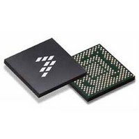
SC900841JVKR2 Freescale Semiconductor, SC900841JVKR2 Datasheet - Page 103

SC900841JVKR2
Manufacturer Part Number
SC900841JVKR2
Description
IC POWER MGT 338-MAPBGA
Manufacturer
Freescale Semiconductor
Specifications of SC900841JVKR2
Applications
PC's, PDA's
Operating Temperature
-40°C ~ 85°C
Mounting Type
Surface Mount
Package / Case
338-TBGA
Input Voltage
2.8 V to 4.4 V
Maximum Operating Temperature
+ 85 C
Minimum Operating Temperature
- 40 C
Lead Free Status / RoHS Status
Lead free / RoHS Compliant
Current - Supply
-
Voltage - Supply
-
Lead Free Status / Rohs Status
Lead free / RoHS Compliant
Available stocks
Company
Part Number
Manufacturer
Quantity
Price
Company:
Part Number:
SC900841JVKR2
Manufacturer:
Freescale Semiconductor
Quantity:
10 000
- Current page: 103 of 192
- Download datasheet (8Mb)
VIMG25
with a P-CH Pass FET. It is high performance, low noise, and
high PSRR, with a low quiescent current and fast transient
response. VIMG25 is actively discharged during shutdown.
Main Features
• Uses V33 or VPWR as the main power supply
• 80 mA maximum continuous output current
• Optimized for a 2.2 µF external filter capacitor with a
Table 57. VIMG25 Register Structure and Bits Description
Analog Integrated Circuit Device Data
Freescale Semiconductor
AOACCTLVIMG25
VIMG25 is a low drop-out (LDO) fully integrated regulator
maximum of 10 mΩ ESR
CTLVIMG25
Reserved
Name
V
OIMG 25
V
33
or V
Bits
2:0
5:3
7:6
C
PWR
C
INIMG
VOUTIMG25
OIMG 25
PVINIMG
GNDIMG
VIMG25 State Control
x0 = Reserved
x1 = Reserved
x2 = Reserved
x3 = Reserved
VIMG25 State Control during AOAC Exit (when the Exit pin is EXITSTBY pin is asserted). These bits will be
initialized by the system SPI controller after power up.
X0 = Do not copy
x1 = Do not copy
x2 = Do not copy
x3 = Do not copy
Reserved
Figure 56. VIMG25 Detailed Internal Block Diagram
VIMG25CNT (ADDR 0x42 - R/W - Default Value: 0x04)
Discharge
V
I
OIMG25
OIMG25
Controller
Z
Output Monitor
_
+
reference ground pin (GNDIMG) with the VIMG28 regulator,
yet each has independent control. Both can be supplied by
either the V33 output voltage (V33) or directly from the VPWR
node, depending on the output voltage selection of LDO
VIMG28.
• Uses an internal pass FET
• The output for each LDO is monitored for over-current
VIMG25 Status/Control Registers and Bits Description
V
REF
VIMG25 shares an input voltage pin (PVINIMG) and a
conditions and under-voltage events
Description
x4 = OFF
x5 = Low Power
x6 = Active
x7 = Active
x4 = OFF
x5 = Low Power
x6 = Active
x7 = Active
AOACCTLVIMG 25
VIMG 25FAULT
CTLVIMG25
FUNCTIONAL DEVICE OPERATION
Interface
SPI
POWER SUPPLIES
900841
103
Related parts for SC900841JVKR2
Image
Part Number
Description
Manufacturer
Datasheet
Request
R
Part Number:
Description:
Ultra-mobile Platform Pmic
Manufacturer:
Freescale Semiconductor, Inc
Datasheet:

Part Number:
Description:
Sc900 Programmable Penta Uldo With Reset And I2c Interface
Manufacturer:
Semtech Corporation
Datasheet:
Part Number:
Description:
Manufacturer:
Freescale Semiconductor, Inc
Datasheet:
Part Number:
Description:
Manufacturer:
Freescale Semiconductor, Inc
Datasheet:
Part Number:
Description:
Manufacturer:
Freescale Semiconductor, Inc
Datasheet:
Part Number:
Description:
Manufacturer:
Freescale Semiconductor, Inc
Datasheet:
Part Number:
Description:
Manufacturer:
Freescale Semiconductor, Inc
Datasheet:
Part Number:
Description:
Manufacturer:
Freescale Semiconductor, Inc
Datasheet:
Part Number:
Description:
Manufacturer:
Freescale Semiconductor, Inc
Datasheet:
Part Number:
Description:
Manufacturer:
Freescale Semiconductor, Inc
Datasheet:
Part Number:
Description:
Manufacturer:
Freescale Semiconductor, Inc
Datasheet:
Part Number:
Description:
Manufacturer:
Freescale Semiconductor, Inc
Datasheet:
Part Number:
Description:
Manufacturer:
Freescale Semiconductor, Inc
Datasheet:
Part Number:
Description:
Manufacturer:
Freescale Semiconductor, Inc
Datasheet:
Part Number:
Description:
Manufacturer:
Freescale Semiconductor, Inc
Datasheet:


