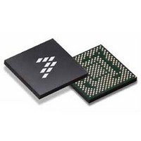
SC900841JVKR2 Freescale Semiconductor, SC900841JVKR2 Datasheet - Page 49

SC900841JVKR2
Manufacturer Part Number
SC900841JVKR2
Description
IC POWER MGT 338-MAPBGA
Manufacturer
Freescale Semiconductor
Specifications of SC900841JVKR2
Applications
PC's, PDA's
Operating Temperature
-40°C ~ 85°C
Mounting Type
Surface Mount
Package / Case
338-TBGA
Input Voltage
2.8 V to 4.4 V
Maximum Operating Temperature
+ 85 C
Minimum Operating Temperature
- 40 C
Lead Free Status / RoHS Status
Lead free / RoHS Compliant
Current - Supply
-
Voltage - Supply
-
Lead Free Status / Rohs Status
Lead free / RoHS Compliant
Available stocks
Company
Part Number
Manufacturer
Quantity
Price
Company:
Part Number:
SC900841JVKR2
Manufacturer:
Freescale Semiconductor
Quantity:
10 000
- Current page: 49 of 192
- Download datasheet (8Mb)
Table 14. VIDEN Selections
= 1.1 V; VNN VBOOT = 0.9 V) settings that the Platform
controller hub sets to the VNN and VCC regulators by a SPI
write to the VNNLATCH and VCCLATCH registers. Once all
of the platform voltage rails are up, the CPU will drive the VID
and VIDEN signals to set the VNN and VCC output voltage to
the appropriate level. The VID and VIDEN signals will go
through the sequence INVALID >> VNN >> INVALID >>
VCC.
PMIC must de-bounce the VID[6:0] and VIDEN[1:0] for 100
to 400 ns. The CPU will hold these signals valid for at least
500 ns. VID signals are disabled from controlling VCC/VNN
unless the VCCP regulator is enabled
normal runtime operation. For the VNN regulator, dynamic
VIDs require the CPU to change the VIDEN signals to
INVALID each time to change the VNN output voltage. The
VCC regulator is different in that it does not require the
VIDEN signals to change to change the VCC output voltage.
If the VIDEN signals are set for VCC (01) the VID signals can
change and the VCC regulator will respond by changing the
output voltage accordingly.
during normal runtime operation when the VIDEN signals are
set to VCC (01). If the VIDEN signals are set to VCC (01), the
VCC regulator must monitor the VID signals, latch any
changes, and change the output voltage setting accordingly.
During normal operation, when the CPU is dynamically
changing the VID setting for the VCC regulator, it will only
change the VID combination by 1 step, which corresponds to
Analog Integrated Circuit Device Data
Freescale Semiconductor
Both VCC and VNN have initial boot voltage (VCC VBOOT
VID[6:0] and VIDEN[1:0] will transition together and the
Both regulators support dynamic VID transitioning during
Figure 13
VIDEN[1:0] Bits
0
0
1
1
shows how the VCC output voltage can change
0
1
0
1
Selection
Unused
Invalid
VCC
VNN
Figure 13. Dynamic VCC Timing Diagram
Table 15. VCC and VNN Latch Register Structure and Bit
a voltage step of ±12.5 mV. During these changes, the VCC
regulator must follow the 25 mV/ms slew rate specification.
dynamic changes to the VNN regulator output voltage require
the VIDEN signals to change to INVALID each time.
Figure 14
during normal runtime operation.
CPU to indicate if the VID bus is addressing VCC or VNN.
They follow the DC Signaling specifications in
reference of 1.05 V (VCCPAOAC)
CPU to indicate the output voltage setting for the VCC and
VNN rails. They follow the DC Signaling specifications in
Table 3
Platform controller hub output driver Impedance is a pull-up
(55 Ω+20%/-55%) and pull-down (55 Ω+20%/-55%).
Motherboard Impedance is 55 Ω±15%. Under extreme
conditions, there could be ringing that cross the 70/30%
threshold, hence the de-bounce requirements. Maximum
leakage current on the VID pins is 100 mA.
in an internal register that will be updated with every VID[6:0]
pin signaling
Reserved
Reserved
VCCVID
VNNVID
Name
The VNN regulator differs from the VCC regulator, in that
The VIDEN[1:0] pins are active high signals driven by the
The VID[6:0] pins are active high signals driven by the
The VID output buffer driver is of the CMOS type. The
VID[6:0] for each of the VCC and VNN rails will be latched
FSLVNNLATCH (ADDR 0x1CA - R - Default Value: 0x7F)
FSLVCCLATCH (ADDR 0x1C9 - R - Default Value: 0x7F)
with a reference of 1.05 V (VCCP)
shows how the VNN output voltage can change
Description
Bits
6:0
6:0
7
7
This register latches an Image of the last
VID[6:0] signals for VCC
Reserved
This register latches an Image of the last
VID[6:0] signals for VNN
Reserved
FUNCTIONAL DEVICE OPERATION
SYSTEM CONTROL INTERFACE
Description
Table 3
with a
900841
49
Related parts for SC900841JVKR2
Image
Part Number
Description
Manufacturer
Datasheet
Request
R
Part Number:
Description:
Ultra-mobile Platform Pmic
Manufacturer:
Freescale Semiconductor, Inc
Datasheet:

Part Number:
Description:
Sc900 Programmable Penta Uldo With Reset And I2c Interface
Manufacturer:
Semtech Corporation
Datasheet:
Part Number:
Description:
Manufacturer:
Freescale Semiconductor, Inc
Datasheet:
Part Number:
Description:
Manufacturer:
Freescale Semiconductor, Inc
Datasheet:
Part Number:
Description:
Manufacturer:
Freescale Semiconductor, Inc
Datasheet:
Part Number:
Description:
Manufacturer:
Freescale Semiconductor, Inc
Datasheet:
Part Number:
Description:
Manufacturer:
Freescale Semiconductor, Inc
Datasheet:
Part Number:
Description:
Manufacturer:
Freescale Semiconductor, Inc
Datasheet:
Part Number:
Description:
Manufacturer:
Freescale Semiconductor, Inc
Datasheet:
Part Number:
Description:
Manufacturer:
Freescale Semiconductor, Inc
Datasheet:
Part Number:
Description:
Manufacturer:
Freescale Semiconductor, Inc
Datasheet:
Part Number:
Description:
Manufacturer:
Freescale Semiconductor, Inc
Datasheet:
Part Number:
Description:
Manufacturer:
Freescale Semiconductor, Inc
Datasheet:
Part Number:
Description:
Manufacturer:
Freescale Semiconductor, Inc
Datasheet:
Part Number:
Description:
Manufacturer:
Freescale Semiconductor, Inc
Datasheet:


