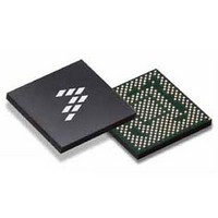
SC900841JVKR2 Freescale Semiconductor, SC900841JVKR2 Datasheet - Page 51

SC900841JVKR2
Manufacturer Part Number
SC900841JVKR2
Description
IC POWER MGT 338-MAPBGA
Manufacturer
Freescale Semiconductor
Specifications of SC900841JVKR2
Applications
PC's, PDA's
Operating Temperature
-40°C ~ 85°C
Mounting Type
Surface Mount
Package / Case
338-TBGA
Input Voltage
2.8 V to 4.4 V
Maximum Operating Temperature
+ 85 C
Minimum Operating Temperature
- 40 C
Lead Free Status / RoHS Status
Lead free / RoHS Compliant
Current - Supply
-
Voltage - Supply
-
Lead Free Status / Rohs Status
Lead free / RoHS Compliant
Available stocks
Company
Part Number
Manufacturer
Quantity
Price
Company:
Part Number:
SC900841JVKR2
Manufacturer:
Freescale Semiconductor
Quantity:
10 000
- Current page: 51 of 192
- Download datasheet (8Mb)
Table 16. Freescale Chipset Communication Signals Pin
V3GPASTTS
pins from the CPU, and if the DVPxVRD bit is set to a '1', the
regulator uses the VNNLATCH and VCCLATCH registers to
set the output voltage.
VNNLATCH and VCCLATCH registers should be ignored.
When the DVPxVRD bit is set to a '1', any changes on the
VID/VIDEN pins from the CPU should be ignored.
switches from using the VID/VIDEN pins to using the
I2S/PCM INTERFACE
Audio.
FREESCALE CHIP SET COMMUNICATION
SIGNALS
between the 900841 and the companion chip, 900842, in
Freescale’s power management solution.
Analog Integrated Circuit Device Data
Freescale Semiconductor
V3GPAEN
Pin Name
V33STTS
V33ISNS
V33EN
When the DVPxVRD bit is set to a '0', any changes to the
As soon as the DVPxVRD bit is set to a '1', the regulator
A detailed description of the I2S interface is provided in
This includes the control and status reporting signal
Functionality
Figure 16. Relationship Between the VID/VIDEN Pins, the DPV1VRD Bit, and VRCOMP Signal
I/O
O
O
I
I
I
V33 Enable output pin
V33 Status input pin. Active low when V33
output is on
Input Interface with the ADC to measure V33
output current
Reserved
Reserved
SCU
Pin Functionality
SCU
SCU
VCCLATCH register, and the output voltage of the regulator
changes to what the VCCLATCH register is set.
VRCOMP signal. The PMIC toggles the VRCOMP signal any
time the DVPxVRD bit is set to a '1' and the output voltage of
the VNN or the VCC regulator changes. If the output voltage
of the VCC/VNN regulator changes and the DVPxVRD bit is
set to a '0', the VRCOMP signal should not toggle. In other
words, VRCOMP only toggles for changes to VCC and VNN
through the SPI registers.
management solution consists of two chips. The 900842
supplies the 3.3 V rail (V33).
outlined above for control and status reporting functions.
chip, by setting the desired voltage regulator control setting in
the 900841 register space. The 900841 in turn uses the
V33EN pin to enable or disable the V33 chip. This transaction
is seamless to the Platform controller hub.
like THERMTRIPB assertion, it can also use the V33EN pin
to turn off the V33 rail. In turn, the V33 rail communicates
back to the 900841 its output voltage status, through the
V33STTS pin, so the 900841 has full visibility on the health of
the 3.3 V rail and can report back to the Platform controller
hub through the VRFAULT Interrupt if V33 has shutdown,
due to a local problem, such as over-temperature.
900841 for sampling by the ADC through the V33ISNS pin.
Figure 16
As explained in
The 900841 interfaces with the 900842 using the signals
The Platform controller hub has full control over the V33
If the 900841 is going through a forced shutdown event,
V33 also sends its output current information to the
SCU
also shows how the PMIC controls the
General
SCU
FUNCTIONAL DEVICE OPERATION
Description, Freescale’s power
SYSTEM CONTROL INTERFACE
900841
51
Related parts for SC900841JVKR2
Image
Part Number
Description
Manufacturer
Datasheet
Request
R
Part Number:
Description:
Ultra-mobile Platform Pmic
Manufacturer:
Freescale Semiconductor, Inc
Datasheet:

Part Number:
Description:
Sc900 Programmable Penta Uldo With Reset And I2c Interface
Manufacturer:
Semtech Corporation
Datasheet:
Part Number:
Description:
Manufacturer:
Freescale Semiconductor, Inc
Datasheet:
Part Number:
Description:
Manufacturer:
Freescale Semiconductor, Inc
Datasheet:
Part Number:
Description:
Manufacturer:
Freescale Semiconductor, Inc
Datasheet:
Part Number:
Description:
Manufacturer:
Freescale Semiconductor, Inc
Datasheet:
Part Number:
Description:
Manufacturer:
Freescale Semiconductor, Inc
Datasheet:
Part Number:
Description:
Manufacturer:
Freescale Semiconductor, Inc
Datasheet:
Part Number:
Description:
Manufacturer:
Freescale Semiconductor, Inc
Datasheet:
Part Number:
Description:
Manufacturer:
Freescale Semiconductor, Inc
Datasheet:
Part Number:
Description:
Manufacturer:
Freescale Semiconductor, Inc
Datasheet:
Part Number:
Description:
Manufacturer:
Freescale Semiconductor, Inc
Datasheet:
Part Number:
Description:
Manufacturer:
Freescale Semiconductor, Inc
Datasheet:
Part Number:
Description:
Manufacturer:
Freescale Semiconductor, Inc
Datasheet:
Part Number:
Description:
Manufacturer:
Freescale Semiconductor, Inc
Datasheet:


