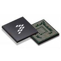
SC900841JVKR2 Freescale Semiconductor, SC900841JVKR2 Datasheet - Page 77

SC900841JVKR2
Manufacturer Part Number
SC900841JVKR2
Description
IC POWER MGT 338-MAPBGA
Manufacturer
Freescale Semiconductor
Specifications of SC900841JVKR2
Applications
PC's, PDA's
Operating Temperature
-40°C ~ 85°C
Mounting Type
Surface Mount
Package / Case
338-TBGA
Input Voltage
2.8 V to 4.4 V
Maximum Operating Temperature
+ 85 C
Minimum Operating Temperature
- 40 C
Lead Free Status / RoHS Status
Lead free / RoHS Compliant
Current - Supply
-
Voltage - Supply
-
Lead Free Status / Rohs Status
Lead free / RoHS Compliant
Available stocks
Company
Part Number
Manufacturer
Quantity
Price
Company:
Part Number:
SC900841JVKR2
Manufacturer:
Freescale Semiconductor
Quantity:
10 000
- Current page: 77 of 192
- Download datasheet (8Mb)
VYMX3G
Buck PWM voltage-mode control DC/DC regulator.
the load conditions. These modes can be set through the SPI
and include a PFM mode, an Automatic Pulse Skipping
mode, and a PWM mode. The above selection is optimized
to maximum battery life based on load conditions.
shutting down.
ADC, and stored in a register for the processor to access.
Table 35. V15CNT Register Structure and Bits Description
Analog Integrated Circuit Device Data
Freescale Semiconductor
AOACCTLV15
This is a 4.0 MHz fully integrated 2-switch synchronous
The switcher can operate in different modes depending on
VYMX3G will be discharged every time the regulator is
The output current is measured internally, digitized by the
CTLV15
SELV15
Name
Bits
2:0
5:3
7:6
V15 State Control
x0 = Reserved
x1 = Reserved
x2 = Reserved
x3 = Reserved
V15 State Control during AOAC Exit (when EXITSTBY pin is asserted). These bits will be initialized by the system SPI
controller after power up
X0 = Do not copy
x1 = Do not copy
x2 = Do not copy
x3 = Do not copy
V15 Output Voltage Selection (FSL Usage Only)
X0 = 1.5 V
x1 = 1.6 V
x2, x3 = Reserved
V
YMX 3G
C
C
INYMX 3G
OYMX 3G
V
L
YMX 3G
PWR
Figure 33. VYMX3G Detailed Internal Block Diagram
PGNDYMX3G
V15CNT (ADDR 0x39 - R/W - Default value: 0x07)
PVINYMX3G
FBYMX3G
SWYMX3G
Internal
Compensation
I
Z1
SENSE 5
Driver
EA
protection purposes. If an over-current condition is detected,
the regulator will limit the current through cycle by cycle
operation and alert the system through the VYMX3GFAULT
signal, which will in turn assert the VRFAULT Interrupt signal.
modules digital core supply and has to different output
voltage settings depending on the application. For WiMAX
applications the output voltage is set to 1.25 V. For 3G
applications the output voltage can be varied between 0.6 to
1.375 V through the Mini-SPI interface. See
COMMs Serial Interface
Z2
Controller
Description
The peak current is sensed internally for over-current
This regulator is used as the advanced communications
x4 = OFF
x5 = PFM
x6 = Automatic Pulse Skipping
x7 = PWM
x4 = OFF
x5 = PFM
x6 = Automatic Pulse Skipping
x7 = PWM
Mini-SPI
DAC
AOACCTLVYMX 3G
VYMX3GFAULT
CTLVYMX3G
SELVYMX 3G
YMX/3G
V
REF
for more details.
Interface
FUNCTIONAL DEVICE OPERATION
SPI
POWER SUPPLIES
Advanced
900841
77
Related parts for SC900841JVKR2
Image
Part Number
Description
Manufacturer
Datasheet
Request
R
Part Number:
Description:
Ultra-mobile Platform Pmic
Manufacturer:
Freescale Semiconductor, Inc
Datasheet:

Part Number:
Description:
Sc900 Programmable Penta Uldo With Reset And I2c Interface
Manufacturer:
Semtech Corporation
Datasheet:
Part Number:
Description:
Manufacturer:
Freescale Semiconductor, Inc
Datasheet:
Part Number:
Description:
Manufacturer:
Freescale Semiconductor, Inc
Datasheet:
Part Number:
Description:
Manufacturer:
Freescale Semiconductor, Inc
Datasheet:
Part Number:
Description:
Manufacturer:
Freescale Semiconductor, Inc
Datasheet:
Part Number:
Description:
Manufacturer:
Freescale Semiconductor, Inc
Datasheet:
Part Number:
Description:
Manufacturer:
Freescale Semiconductor, Inc
Datasheet:
Part Number:
Description:
Manufacturer:
Freescale Semiconductor, Inc
Datasheet:
Part Number:
Description:
Manufacturer:
Freescale Semiconductor, Inc
Datasheet:
Part Number:
Description:
Manufacturer:
Freescale Semiconductor, Inc
Datasheet:
Part Number:
Description:
Manufacturer:
Freescale Semiconductor, Inc
Datasheet:
Part Number:
Description:
Manufacturer:
Freescale Semiconductor, Inc
Datasheet:
Part Number:
Description:
Manufacturer:
Freescale Semiconductor, Inc
Datasheet:
Part Number:
Description:
Manufacturer:
Freescale Semiconductor, Inc
Datasheet:


