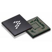
SC900841JVKR2 Freescale Semiconductor, SC900841JVKR2 Datasheet - Page 2

SC900841JVKR2
Manufacturer Part Number
SC900841JVKR2
Description
IC POWER MGT 338-MAPBGA
Manufacturer
Freescale Semiconductor
Specifications of SC900841JVKR2
Applications
PC's, PDA's
Operating Temperature
-40°C ~ 85°C
Mounting Type
Surface Mount
Package / Case
338-TBGA
Input Voltage
2.8 V to 4.4 V
Maximum Operating Temperature
+ 85 C
Minimum Operating Temperature
- 40 C
Lead Free Status / RoHS Status
Lead free / RoHS Compliant
Current - Supply
-
Voltage - Supply
-
Lead Free Status / Rohs Status
Lead free / RoHS Compliant
Available stocks
Company
Part Number
Manufacturer
Quantity
Price
Company:
Part Number:
SC900841JVKR2
Manufacturer:
Freescale Semiconductor
Quantity:
10 000
- Current page: 2 of 192
- Download datasheet (8Mb)
POWER DISSIPATION
exceed the maximum junction temperature. Depending on
the operating ambient temperature and the total internal
dissipation this limit can be exceeded.
overheating, the 900841 provides a thermal management
system that protects against overheating. This protection
should be considered as a fail-safe mechanism, and the
application design should initiate thermal shutdown under
normal conditions. Reference
details.
2
900841
Table 1. Maximum Ratings
damage to the device. The detailed maximum voltage rating per pin can be found in the pin list section.
ELECTRICAL CHARACTERISTICS
MAXIMUM RATINGS
ELECTRICAL RATINGS
THERMAL RATINGS
Notes
Charger Input Voltage
LCD Backlight Circuitry Voltage
Battery Voltage
Coin Cell Voltage
ESD Rating, All Pins, Human Body Model (HBM)
ESD Rating, All Pins, Charge Device Model (CDM)
Ambient Operating Temperature Range
Operating Junction Temperature Range
Storage Temperature Range
Peak Package Reflow Temperature
During operation, the temperature of the die must not
To optimize the thermal management scheme and avoid
All voltages are with respect to ground, unless otherwise noted. Exceeding these ratings may cause malfunction or permanent
1.
2.
3.
4.
Pin soldering temperature limit is for 10 seconds maximum duration. Not designed for immersion soldering. Exceeding these limits may
cause a malfunction or permanent damage to the device.
Freescale's Package Reflow capability meets the Pb-free requirements for JEDEC standard J-STD-020C, for Peak Package Reflow
Temperature and Moisture Sensitivity Levels (MSL)
ESD testing is performed in accordance with the Human Body Model (HBM) (CZAP = 100 pF, RZAP = 1500 Ω), and the Charge Device
Model (CDM), Robotic (CZAP = 4.0 pF).
All pins meet 500 V CDM except VCOREREF.
Thermal Management
(1),
(2)
Ratings
ELECTRICAL CHARACTERISTICS
(3)
(3),
(4)
MAXIMUM RATINGS
for more
POWER CONSUMPTION
specifications in the various system and device states. For
each entry in the table, the component is assumed to be
configured for driving purely capacitive loads, and the
voltages listed in each entry are nominal output voltages.
state. The device will spend less than 150 µs in this state
before V15 starts to turn on, upon detection of a valid USB
device or valid battery.
Table 2
Note that the “Soft Mechanical Off” state is a transitional
defines the maximum power consumption
V
V
Symbol
ESDHBM
ESDCDM
T
T
PPRT
T
T
Analog Integrated Circuit Device Data
-
-
-
-
ST
A
J
Freescale Semiconductor
-0.3 to +4.4
-0.3 to +3.6
-30 to +125
-65 to +150
-0.3 to +20
-0.3 to +28
-40 to +85
±2000
Value
±450
260
Unit
°
°
°
°
V
V
V
V
V
V
C
C
C
C
Related parts for SC900841JVKR2
Image
Part Number
Description
Manufacturer
Datasheet
Request
R
Part Number:
Description:
Ultra-mobile Platform Pmic
Manufacturer:
Freescale Semiconductor, Inc
Datasheet:

Part Number:
Description:
Sc900 Programmable Penta Uldo With Reset And I2c Interface
Manufacturer:
Semtech Corporation
Datasheet:
Part Number:
Description:
Manufacturer:
Freescale Semiconductor, Inc
Datasheet:
Part Number:
Description:
Manufacturer:
Freescale Semiconductor, Inc
Datasheet:
Part Number:
Description:
Manufacturer:
Freescale Semiconductor, Inc
Datasheet:
Part Number:
Description:
Manufacturer:
Freescale Semiconductor, Inc
Datasheet:
Part Number:
Description:
Manufacturer:
Freescale Semiconductor, Inc
Datasheet:
Part Number:
Description:
Manufacturer:
Freescale Semiconductor, Inc
Datasheet:
Part Number:
Description:
Manufacturer:
Freescale Semiconductor, Inc
Datasheet:
Part Number:
Description:
Manufacturer:
Freescale Semiconductor, Inc
Datasheet:
Part Number:
Description:
Manufacturer:
Freescale Semiconductor, Inc
Datasheet:
Part Number:
Description:
Manufacturer:
Freescale Semiconductor, Inc
Datasheet:
Part Number:
Description:
Manufacturer:
Freescale Semiconductor, Inc
Datasheet:
Part Number:
Description:
Manufacturer:
Freescale Semiconductor, Inc
Datasheet:
Part Number:
Description:
Manufacturer:
Freescale Semiconductor, Inc
Datasheet:


