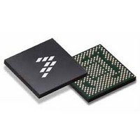
SC900841JVKR2 Freescale Semiconductor, SC900841JVKR2 Datasheet - Page 32

SC900841JVKR2
Manufacturer Part Number
SC900841JVKR2
Description
IC POWER MGT 338-MAPBGA
Manufacturer
Freescale Semiconductor
Specifications of SC900841JVKR2
Applications
PC's, PDA's
Operating Temperature
-40°C ~ 85°C
Mounting Type
Surface Mount
Package / Case
338-TBGA
Input Voltage
2.8 V to 4.4 V
Maximum Operating Temperature
+ 85 C
Minimum Operating Temperature
- 40 C
Lead Free Status / RoHS Status
Lead free / RoHS Compliant
Current - Supply
-
Voltage - Supply
-
Lead Free Status / Rohs Status
Lead free / RoHS Compliant
Available stocks
Company
Part Number
Manufacturer
Quantity
Price
Company:
Part Number:
SC900841JVKR2
Manufacturer:
Freescale Semiconductor
Quantity:
10 000
- Current page: 32 of 192
- Download datasheet (8Mb)
Table 5. SC900841 Pin Description
32
900841
FUNCTIONAL DESCRIPTION
GENERAL DESCRIPTION
PGNDYMX3G
PGNDYMXPA
YMXPAGTIN
V3GPASTTS
PVINYMX3G
Node Name
PGNDBKLT
SWYMX3G
SWYMXPA
PGNDOTG
YMXPAGT
VOUTCCA
FBYMX3G
FBYMXPA
V3GPAEN
OTGGTIN
VOUTBG
SWBKLT
PVIN1P8
GND1P8
SWOTG
FBBKLT
OTGGT
FBOTG
FBCCA
HIPWRGND
HIPWRGND
HIPWRGND
HIPWRGND
MDPWR
MDPWR
MDPWR
MDPWR
LOPWR
LOPWR
LOPWR
HIPWR
HIPWR
HIPWR
HIPWR
HIPWR
SGNL
SGNL
SGNL
SGNL
SGNL
SGNL
SGNL
Type
GND
VBKLT - 5s3p (Backlight) and 5s1p (Camera Scene) / 120 mA Boost
I/O
O
-
-
-
-
-
-
-
-
-
-
-
-
-
-
-
-
-
I
I
I
I
I
I
VYMX3G - (YMX: 1.25 V or 3G: 0.6 V-1.375 V) / 1.0 A BUCK
Rating
4.8 V
4.8 V
3.6 V
5.5 V
5.5 V
5.5 V
5.5 V
2.5 V
2.5 V
5.5 V
5.5 V
5.5 V
5.5 V
3.6 V
2.5 V
2.5 V
2.5 V
26 V
26 V
-
-
-
-
-
Balls
# of
VYMXPA - 4.2 V / 0.7 A Boost
2
2
2
1
3
3
1
1
1
1
1
2
2
1
1
1
2
2
1
1
1
1
1
1
V3GPA Interface (Reserved)
VOTG - 5.0 V / 0.35 A Boost
VCCA - 1.5 V/150 mA LDO
VBG - 1.25 V/2 mA LDO
AD12, AF12, AH12 Power Ground
AE11, AG11, AJ11 Switch Node
BGA Location
W27, W29
U27, U29
V26, V28
Y26, Y28
R1, R3
T6, T8
T2, T4
AA13
AA15
AA23
AA25
W13
W21
W23
U21
N13
V24
U9
D6
D2
C3
E7
Power Supply Input
Switch Node
Power Ground
Output Voltage Feedback Input
Output Voltage Feedback Input
Gate Drive Input for VYMXPA isolation FET
Gate Driver for external switch if output isolation is required
V3GPA Enable output pin. Reserved
V3GPA Status input pin. Reserved
Switch Node
Power Ground
Output Voltage Feedback Input
Gate Drive Input for VOTG Isolation FET
Gate Driver for external switch if output isolation is required
Switch Node
Power Ground
Output Voltage Feedback Input
Power Supply Input, shared by VBG and VCCA
Ground Reference
VBG Output Voltage Node
VCCA Output Voltage Node
VCCA Output Voltage Feedback Input
Analog Integrated Circuit Device Data
Pin Description
Freescale Semiconductor
Related parts for SC900841JVKR2
Image
Part Number
Description
Manufacturer
Datasheet
Request
R
Part Number:
Description:
Ultra-mobile Platform Pmic
Manufacturer:
Freescale Semiconductor, Inc
Datasheet:

Part Number:
Description:
Sc900 Programmable Penta Uldo With Reset And I2c Interface
Manufacturer:
Semtech Corporation
Datasheet:
Part Number:
Description:
Manufacturer:
Freescale Semiconductor, Inc
Datasheet:
Part Number:
Description:
Manufacturer:
Freescale Semiconductor, Inc
Datasheet:
Part Number:
Description:
Manufacturer:
Freescale Semiconductor, Inc
Datasheet:
Part Number:
Description:
Manufacturer:
Freescale Semiconductor, Inc
Datasheet:
Part Number:
Description:
Manufacturer:
Freescale Semiconductor, Inc
Datasheet:
Part Number:
Description:
Manufacturer:
Freescale Semiconductor, Inc
Datasheet:
Part Number:
Description:
Manufacturer:
Freescale Semiconductor, Inc
Datasheet:
Part Number:
Description:
Manufacturer:
Freescale Semiconductor, Inc
Datasheet:
Part Number:
Description:
Manufacturer:
Freescale Semiconductor, Inc
Datasheet:
Part Number:
Description:
Manufacturer:
Freescale Semiconductor, Inc
Datasheet:
Part Number:
Description:
Manufacturer:
Freescale Semiconductor, Inc
Datasheet:
Part Number:
Description:
Manufacturer:
Freescale Semiconductor, Inc
Datasheet:
Part Number:
Description:
Manufacturer:
Freescale Semiconductor, Inc
Datasheet:


