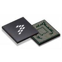
SC900841JVKR2 Freescale Semiconductor, SC900841JVKR2 Datasheet - Page 108

SC900841JVKR2
Manufacturer Part Number
SC900841JVKR2
Description
IC POWER MGT 338-MAPBGA
Manufacturer
Freescale Semiconductor
Specifications of SC900841JVKR2
Applications
PC's, PDA's
Operating Temperature
-40°C ~ 85°C
Mounting Type
Surface Mount
Package / Case
338-TBGA
Input Voltage
2.8 V to 4.4 V
Maximum Operating Temperature
+ 85 C
Minimum Operating Temperature
- 40 C
Lead Free Status / RoHS Status
Lead free / RoHS Compliant
Current - Supply
-
Voltage - Supply
-
Lead Free Status / Rohs Status
Lead free / RoHS Compliant
Available stocks
Company
Part Number
Manufacturer
Quantity
Price
Company:
Part Number:
SC900841JVKR2
Manufacturer:
Freescale Semiconductor
Quantity:
10 000
- Current page: 108 of 192
- Download datasheet (8Mb)
Table 62. Power Switches Control Registers Structure and Bits Description
Table 63. V33 Control Register Structure and Bits Description
STAND ALONE VOLTAGE SUPPLIES.
V33
Buck-boost PWM voltage mode control DC/DC regulator.
chip. See
900842 datasheet.
more details about how the 900841 communicates to this
standalone chip for complete system operation.
POWER SUPPLY REGISTER MASK
the need for the system controller to do read-modify-write
cycles. The mask register is shown in
108
Table 64. Mask Register
900841
FUNCTIONAL DEVICE OPERATION
POWER SUPPLIES
AOACCTLVGYMX33
AOACCTLV33
This is a 1.625 MHz fully integrated 4-switch synchronous
This rail is implemented through an external standalone
A separate specification is provided for this rail in the
Reference
Mask writes to the power supply registers, in order to avoid
Reserved
CTLV33
Reserved
Name
Register name
PWRMASK
General
Freescale Chip set Communication Signals
Description.
Bits
2:0
5:3
7:6
5:3
7:6
V33 State Control
x0 = Reserved
x1 = Reserved
x2 = Reserved
x3 = Reserved
V33 State Control during AOAC Exit (when Exit pin is EXITSTBY pin is asserted). These bits will be initialized by
the system SPI controller after power up.
X0 = Do not copy
x1 = Do not copy
x2 = Do not copy
x3 = Do not copy
Reserved
VYMXGPS33 State Control during AOAC Exit (when Exit pin is EXITSTBY pin is asserted). These bits will be
initialized by the system SPI controller after power up.
X0 = Do not copy
x1 = Do not copy
x2 = Do not copy
x3 = Do not copy
Reserved
ADDR
0x34
Table
V33CNT (ADDR 0x3A - R/W - Default Value: 0x24)
R/W
R/W
64.
M7
D7
for
M6
D6
Main Features
• Uses the V
• It is used as a pre-regulator to many LDO and Switch rails
• Uses Integrated MOSFETs
• 1.625 MHz switching frequency
• Output can be discharged
• Output Current Sensing with over-current protection
• Uses internal compensation
• Gate drive circuits are supplied directly from VPWR
V33 Status/Control Registers and Bits Description
M5
D5
for enhanced efficiency and reduced thermal dissipation. It
also supplies power to rails in Platform controller hub and
the platform
Description
M4
x4 = OFF
x5 = Low power
x6 = PWM
x7 = PWM
x4 = OFF
x5 = Low power
x6 = PWM
x7 = PWM
D4
x4 = OFF
x5 = Low Power
x6 = Active
x7 = Active
PWR
rail as its power supply
M3
D3
Analog Integrated Circuit Device Data
M2
D2
Freescale Semiconductor
M1
D1
D0
M0
initial
0x00
Related parts for SC900841JVKR2
Image
Part Number
Description
Manufacturer
Datasheet
Request
R
Part Number:
Description:
Ultra-mobile Platform Pmic
Manufacturer:
Freescale Semiconductor, Inc
Datasheet:

Part Number:
Description:
Sc900 Programmable Penta Uldo With Reset And I2c Interface
Manufacturer:
Semtech Corporation
Datasheet:
Part Number:
Description:
Manufacturer:
Freescale Semiconductor, Inc
Datasheet:
Part Number:
Description:
Manufacturer:
Freescale Semiconductor, Inc
Datasheet:
Part Number:
Description:
Manufacturer:
Freescale Semiconductor, Inc
Datasheet:
Part Number:
Description:
Manufacturer:
Freescale Semiconductor, Inc
Datasheet:
Part Number:
Description:
Manufacturer:
Freescale Semiconductor, Inc
Datasheet:
Part Number:
Description:
Manufacturer:
Freescale Semiconductor, Inc
Datasheet:
Part Number:
Description:
Manufacturer:
Freescale Semiconductor, Inc
Datasheet:
Part Number:
Description:
Manufacturer:
Freescale Semiconductor, Inc
Datasheet:
Part Number:
Description:
Manufacturer:
Freescale Semiconductor, Inc
Datasheet:
Part Number:
Description:
Manufacturer:
Freescale Semiconductor, Inc
Datasheet:
Part Number:
Description:
Manufacturer:
Freescale Semiconductor, Inc
Datasheet:
Part Number:
Description:
Manufacturer:
Freescale Semiconductor, Inc
Datasheet:
Part Number:
Description:
Manufacturer:
Freescale Semiconductor, Inc
Datasheet:


