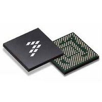
SC900841JVKR2 Freescale Semiconductor, SC900841JVKR2 Datasheet - Page 70

SC900841JVKR2
Manufacturer Part Number
SC900841JVKR2
Description
IC POWER MGT 338-MAPBGA
Manufacturer
Freescale Semiconductor
Specifications of SC900841JVKR2
Applications
PC's, PDA's
Operating Temperature
-40°C ~ 85°C
Mounting Type
Surface Mount
Package / Case
338-TBGA
Input Voltage
2.8 V to 4.4 V
Maximum Operating Temperature
+ 85 C
Minimum Operating Temperature
- 40 C
Lead Free Status / RoHS Status
Lead free / RoHS Compliant
Current - Supply
-
Voltage - Supply
-
Lead Free Status / Rohs Status
Lead free / RoHS Compliant
Available stocks
Company
Part Number
Manufacturer
Quantity
Price
Company:
Part Number:
SC900841JVKR2
Manufacturer:
Freescale Semiconductor
Quantity:
10 000
- Current page: 70 of 192
- Download datasheet (8Mb)
• Loss-Less Output Current Sensing with over-current
• Uses internal compensation
• Gate drive circuits are supplied directly from VPWR
VCC Status/Control Registers and Bits Description
default state for each of these registers.
70
900841
Table 31. VCC Status Registers Structure and Bits Description
FUNCTIONAL DEVICE OPERATION
POWER SUPPLIES
AOACCTLVCC 5:3
protection
Reference the register map for read/write conditions and
DVP1VRD
Reserved
CTLVCC
VIDVCC
Name
Bits
2:0
7:6
6:0
7
VCC State Control
x0 = Reserved
x1 = Reserved
x2 = Reserved
x3 = Reserved
VCC State Control during AOAC Exit (when Exit pin is EXITSTBY pin is asserted). These bits will be initialized by the
system SPI controller after power up.
X0 = Do not copy
x1 = Do not copy
x2 = Do not copy
x3 = Do not copy
Reserved
VID VCC Control Through SPI. Signal codes are identical to the VID signal codes. Reference
details
VCC Register override enable bit.
X0 = VCC VID control follows the external pins
x1 = VCC VID control follows the VIDVCC control register bits
VCCLATCH (ADDR 0X32 - R/W - Default value: 0x7F)
VCCCNT (ADDR 0x35 - R/W - Default Value: 0x24)
Figure 24. VCC Efficiency Curve
Efficiency Curves
PWM mode, based on the recommended external
component values and typical output voltage of 1.2 V. 3.0 V
≤ VPWR ≤ 4.4 V.
Description
The efficiency curves in
x4 = OFF
x5 = PFM
x6 = Automatic Pulse Skipping
x7 = PWM
x4 = OFF
x5 = PFM
x6 = Automatic Pulse Skipping
x7 = PWM
Analog Integrated Circuit Device Data
Figure 24
Freescale Semiconductor
are calculated under
Figures 15
for more
Related parts for SC900841JVKR2
Image
Part Number
Description
Manufacturer
Datasheet
Request
R
Part Number:
Description:
Ultra-mobile Platform Pmic
Manufacturer:
Freescale Semiconductor, Inc
Datasheet:

Part Number:
Description:
Sc900 Programmable Penta Uldo With Reset And I2c Interface
Manufacturer:
Semtech Corporation
Datasheet:
Part Number:
Description:
Manufacturer:
Freescale Semiconductor, Inc
Datasheet:
Part Number:
Description:
Manufacturer:
Freescale Semiconductor, Inc
Datasheet:
Part Number:
Description:
Manufacturer:
Freescale Semiconductor, Inc
Datasheet:
Part Number:
Description:
Manufacturer:
Freescale Semiconductor, Inc
Datasheet:
Part Number:
Description:
Manufacturer:
Freescale Semiconductor, Inc
Datasheet:
Part Number:
Description:
Manufacturer:
Freescale Semiconductor, Inc
Datasheet:
Part Number:
Description:
Manufacturer:
Freescale Semiconductor, Inc
Datasheet:
Part Number:
Description:
Manufacturer:
Freescale Semiconductor, Inc
Datasheet:
Part Number:
Description:
Manufacturer:
Freescale Semiconductor, Inc
Datasheet:
Part Number:
Description:
Manufacturer:
Freescale Semiconductor, Inc
Datasheet:
Part Number:
Description:
Manufacturer:
Freescale Semiconductor, Inc
Datasheet:
Part Number:
Description:
Manufacturer:
Freescale Semiconductor, Inc
Datasheet:
Part Number:
Description:
Manufacturer:
Freescale Semiconductor, Inc
Datasheet:


