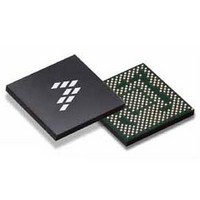
SC900841JVKR2 Freescale Semiconductor, SC900841JVKR2 Datasheet - Page 166

SC900841JVKR2
Manufacturer Part Number
SC900841JVKR2
Description
IC POWER MGT 338-MAPBGA
Manufacturer
Freescale Semiconductor
Specifications of SC900841JVKR2
Applications
PC's, PDA's
Operating Temperature
-40°C ~ 85°C
Mounting Type
Surface Mount
Package / Case
338-TBGA
Input Voltage
2.8 V to 4.4 V
Maximum Operating Temperature
+ 85 C
Minimum Operating Temperature
- 40 C
Lead Free Status / RoHS Status
Lead free / RoHS Compliant
Current - Supply
-
Voltage - Supply
-
Lead Free Status / Rohs Status
Lead free / RoHS Compliant
Available stocks
Company
Part Number
Manufacturer
Quantity
Price
Company:
Part Number:
SC900841JVKR2
Manufacturer:
Freescale Semiconductor
Quantity:
10 000
- Current page: 166 of 192
- Download datasheet (8Mb)
Table 110. ADC Control Registers Structure and Bits Description
166
900841
FUNCTIONAL DEVICE OPERATION
ADC SUBSYSTEM
ADEXGAIN10
ADEXGAIN11
ADEXGAIN12
ADEXGAIN13
ADEXGAIN14
ADEXGAIN15
ADEXGAIN16
PENDETEN
CCCLEAR
ADSTRT
ADSLP
Name
CCEN
ADEN
Bits
2:0
3
4
5
6
7
0
1
2
3
4
5
6
ADC sleep time before starting another cycle
x0 = Continuous Loop
x1 = 4.5 ms
x2 = 9.0 ms
x3 = 13.5 ms
Coulomb Counter Enable
x0 = Disable
x1 = Enable
Coulomb Counter Reset Enable
x0 = Do not reset CC
x1 = CC reset
Enable Touch Screen Pen Detect Bias
x0 = Disabled
x1 = Enabled
ADC Round Robin Start Signal
x0 = Stop round robin after the current cycle
x1 = Start round robin
Bring the ADC out of low power state, this overrides wake from sleep
x0 = Disable in low power
x1 = Enable at full power
Gain bit for ADC channel 10, ignore when touch screen is biased
x0 = x1 (0-2.0 V input range)
x1 = x10 (0-200 mV input range)
Gain bit for ADC channel 11, ignore when touch screen is biased
x0 = x1 (0-2.0 V input range)
x1 = x10 (0-200 mV input range)
Gain bit for ADC channel 12, ignore when touch screen is biased
x0 = x1 (0-2.0 V input range)
x1 = x10 (0-200 mV input range)
Gain bit for ADC channel 13, ignore when touch screen is biased
x0 = x1 (0-2.0 V input range)
x1 = x10 (0-200 mV input range)
Gain bit for ADC channel 14
x0 = x1 (0-2.0 V input range)
x1 = x10 (0-200 mV input range)
Gain bit for ADC channel 15
x0 = x1 (0-2.0 V input range)
x1 = x10 (0-200 mV input range)
Gain bit for ADC channel 16
x0 = x1 (0-2.0 V input range)
x1 = x10 (0-200 mV input range)
ADCCNTL2 (ADDR 0x61 - R/W -Default Value: 0x00)
ADCCNTL3 (ADDR 0x62 - R/W -Default Value: 0x00)
Description
x4 = 18 ms
x5 = 22.5 ms
x6 = 27 ms
x7 = No Loop
Analog Integrated Circuit Device Data
Freescale Semiconductor
Related parts for SC900841JVKR2
Image
Part Number
Description
Manufacturer
Datasheet
Request
R
Part Number:
Description:
Ultra-mobile Platform Pmic
Manufacturer:
Freescale Semiconductor, Inc
Datasheet:

Part Number:
Description:
Sc900 Programmable Penta Uldo With Reset And I2c Interface
Manufacturer:
Semtech Corporation
Datasheet:
Part Number:
Description:
Manufacturer:
Freescale Semiconductor, Inc
Datasheet:
Part Number:
Description:
Manufacturer:
Freescale Semiconductor, Inc
Datasheet:
Part Number:
Description:
Manufacturer:
Freescale Semiconductor, Inc
Datasheet:
Part Number:
Description:
Manufacturer:
Freescale Semiconductor, Inc
Datasheet:
Part Number:
Description:
Manufacturer:
Freescale Semiconductor, Inc
Datasheet:
Part Number:
Description:
Manufacturer:
Freescale Semiconductor, Inc
Datasheet:
Part Number:
Description:
Manufacturer:
Freescale Semiconductor, Inc
Datasheet:
Part Number:
Description:
Manufacturer:
Freescale Semiconductor, Inc
Datasheet:
Part Number:
Description:
Manufacturer:
Freescale Semiconductor, Inc
Datasheet:
Part Number:
Description:
Manufacturer:
Freescale Semiconductor, Inc
Datasheet:
Part Number:
Description:
Manufacturer:
Freescale Semiconductor, Inc
Datasheet:
Part Number:
Description:
Manufacturer:
Freescale Semiconductor, Inc
Datasheet:
Part Number:
Description:
Manufacturer:
Freescale Semiconductor, Inc
Datasheet:


