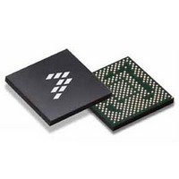
SC900841JVKR2 Freescale Semiconductor, SC900841JVKR2 Datasheet - Page 20

SC900841JVKR2
Manufacturer Part Number
SC900841JVKR2
Description
IC POWER MGT 338-MAPBGA
Manufacturer
Freescale Semiconductor
Specifications of SC900841JVKR2
Applications
PC's, PDA's
Operating Temperature
-40°C ~ 85°C
Mounting Type
Surface Mount
Package / Case
338-TBGA
Input Voltage
2.8 V to 4.4 V
Maximum Operating Temperature
+ 85 C
Minimum Operating Temperature
- 40 C
Lead Free Status / RoHS Status
Lead free / RoHS Compliant
Current - Supply
-
Voltage - Supply
-
Lead Free Status / Rohs Status
Lead free / RoHS Compliant
Available stocks
Company
Part Number
Manufacturer
Quantity
Price
Company:
Part Number:
SC900841JVKR2
Manufacturer:
Freescale Semiconductor
Quantity:
10 000
- Current page: 20 of 192
- Download datasheet (8Mb)
Table 3. Static Electrical Characteristics
noted. Typical values are characterized at V
20
900841
ELECTRICAL CHARACTERISTICS
STATIC ELECTRICAL CHARACTERISTICS
ADC ELECTRICAL CHARACTERISTICS
BATTERY CURRENT READING
BATTERY THERMISTOR INTERFACE TARGET
COULOMB COUNTER
Notes
Conversion Current
OFF Supply Current
Converter Reference Voltage
Integral Nonlinearity (Rs = 5.0 kΩ maximum)
Differential Nonlinearity (Rs = 5.0 kΩ maximum)
Zero Scale Error (Offset) (Rs = 5.0 kΩ maximum)
Full Scale Error (Gain) (Rs = 5.0 kΩ maximum)
Drift Over Temperature
Source Impedance
Input Buffer Input Range
Amplifier
Amplifier Offset
Sense Resistor
Thermistor Input Range
Internal Current Source
Absolute Resistance Measurement Inaccuracy Over Temperature
Battery Removal Detection Threshold
Sense Resistor R
Sense Current though R
Quiescent Current Consumption
Resolution (1LSB Increment in CCOUT with ONEC=1)
10.
T
6.
7.
8.
9.
A
No Bypass Capacitor at Input
Bypass Capacitor at Input of (10 nF)
= -40 °C to 85 °C, V
Rs represents a possible external series resistor between the voltage source and the ADIN input.
Refer to
Amplifier bias current accounted for in overall ADC current drain
This is equivalent to a 10 kΩ pull-up and a 10 kΩ thermistor at -35°C
At room temperature
(8)
Gain
Table 96
CC
CC
for analog valid input range and input buffer range characteristics for each ADC Channel
(7)
PWR
Characteristic
= 3.0 to 4.4 V, typical external component values, and full load current range, unless otherwise
(9)
(6)
(6),
PWR
(6)
(6)
(10)
= 3.6 V and 25 °C.
Symbol
-
-
-
-
-
-
-
-
-
-
-
-
-
-
-
-
-
-
-
-
-
+/-1.0
0.02
Min
-2.0
2.0
19
Analog Integrated Circuit Device Data
-
-
-
-
-
-
-
-
-
-
-
-
-
-
-
-
31/32*
366.2
V
Typ
2.4
20
20
20
10
20
10
NTC
-
-
-
-
-
-
-
-
-
-
-
-
Freescale Semiconductor
+/-3000
Max
±3.0
±1.0
±2.0
100
1.2
1.0
5.0
2.4
2.0
10
11
30
21
20
-
-
-
-
-
-
-
Unit
LSB
LSB
LSB
LSB
LSB
mA
mV
mΩ
mΩ
mA
μA
kΩ
kΩ
μA
μA
μC
%
V
V
V
k
-
Related parts for SC900841JVKR2
Image
Part Number
Description
Manufacturer
Datasheet
Request
R
Part Number:
Description:
Ultra-mobile Platform Pmic
Manufacturer:
Freescale Semiconductor, Inc
Datasheet:

Part Number:
Description:
Sc900 Programmable Penta Uldo With Reset And I2c Interface
Manufacturer:
Semtech Corporation
Datasheet:
Part Number:
Description:
Manufacturer:
Freescale Semiconductor, Inc
Datasheet:
Part Number:
Description:
Manufacturer:
Freescale Semiconductor, Inc
Datasheet:
Part Number:
Description:
Manufacturer:
Freescale Semiconductor, Inc
Datasheet:
Part Number:
Description:
Manufacturer:
Freescale Semiconductor, Inc
Datasheet:
Part Number:
Description:
Manufacturer:
Freescale Semiconductor, Inc
Datasheet:
Part Number:
Description:
Manufacturer:
Freescale Semiconductor, Inc
Datasheet:
Part Number:
Description:
Manufacturer:
Freescale Semiconductor, Inc
Datasheet:
Part Number:
Description:
Manufacturer:
Freescale Semiconductor, Inc
Datasheet:
Part Number:
Description:
Manufacturer:
Freescale Semiconductor, Inc
Datasheet:
Part Number:
Description:
Manufacturer:
Freescale Semiconductor, Inc
Datasheet:
Part Number:
Description:
Manufacturer:
Freescale Semiconductor, Inc
Datasheet:
Part Number:
Description:
Manufacturer:
Freescale Semiconductor, Inc
Datasheet:
Part Number:
Description:
Manufacturer:
Freescale Semiconductor, Inc
Datasheet:


