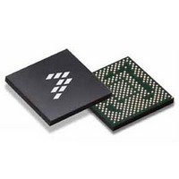
SC900841JVKR2 Freescale Semiconductor, SC900841JVKR2 Datasheet - Page 106

SC900841JVKR2
Manufacturer Part Number
SC900841JVKR2
Description
IC POWER MGT 338-MAPBGA
Manufacturer
Freescale Semiconductor
Specifications of SC900841JVKR2
Applications
PC's, PDA's
Operating Temperature
-40°C ~ 85°C
Mounting Type
Surface Mount
Package / Case
338-TBGA
Input Voltage
2.8 V to 4.4 V
Maximum Operating Temperature
+ 85 C
Minimum Operating Temperature
- 40 C
Lead Free Status / RoHS Status
Lead free / RoHS Compliant
Current - Supply
-
Voltage - Supply
-
Lead Free Status / Rohs Status
Lead free / RoHS Compliant
Available stocks
Company
Part Number
Manufacturer
Quantity
Price
Company:
Part Number:
SC900841JVKR2
Manufacturer:
Freescale Semiconductor
Quantity:
10 000
- Current page: 106 of 192
- Download datasheet (8Mb)
Table 60. VSDIO Control Register Structure and Bits Description
VSDIO
uses an external P-CH pass FET in Switch mode, and internal
pass FET on LDO mode.
1.8 V, and as a switch when its output voltage is set to 3.3 V. It
MAIN FEATURES
• Uses V33 as the main power supply
• 215 mA maximum continuous output current
• Optimized for a 2.2 µF external filter capacitor with a
106
AOACCTLVSDIO
900841
FUNCTIONAL DEVICE OPERATION
POWER SUPPLIES
VSDIO is a combo low drop-out (LDO) and power switch. It
VSDIO serves as an LDO when its output voltage is set to
maximum of 10 mΩ ESR
CTLVSDIO
SELVSDIO
Name
V
OSDIO
C
C
OSDIO
INSDIO
Bits
2:0
5:3
7:6
VSDIO State Control
x0 = Reserved
x1 = Reserved
x2 = Reserved
x3 = Reserved
VSDIO State Control during AOAC Exit (when Exit pin is EXITSTBY pin is asserted). These bits will be initialized by
the system SPI controller after power up.
X0 = Do not copy
x1 = Do not copy
x2 = Do not copy
x3 = Do not copy
VSDIO output voltage selections:
X0 = 1.8 V
x1 = 3.3 V
x2 = Reserved
x3 = Reserved
V
33
M
FBSDIO
SDIOGT
SDIO
Figure 59. VSDIO Detailed Internal Block Diagram
VSDIOCNT (ADDR 0x4D - R/W - Default Value: 0x64)
Discharge
V
OCCP
LDO/Switch
Controller
Z
Output Monitor
_
+
takes its input voltage directly from the V33 output voltage node
(V33).
powered up to 3.3 V. If the card is detected to be a low voltage
card, then the rail will be shutdown, configured as 1.8 V, and
then turned on.
• Uses an internal pass FET on LDO mode, and external pass
• The output is monitored for under-voltage and overcurrent
VSDIO Status/Control Registers and Bits Description
V
REF
VSDIO supplies the SDIO card module. The card is initially
VSDIO will be actively discharged during shutdown.
FET on Switch mode.
conditions in LDO mode.
Description
x4 = OFF
x5 = Low Power
x6 = Active
x7 = Active
x4 = OFF
x5 = Low Power
x6 = Active
x7 = Active
AOACCTLVSDIO
VSDIOFAULT
CTLVSDIO
SELVSDIO
Analog Integrated Circuit Device Data
Interface
SPI
Freescale Semiconductor
Related parts for SC900841JVKR2
Image
Part Number
Description
Manufacturer
Datasheet
Request
R
Part Number:
Description:
Ultra-mobile Platform Pmic
Manufacturer:
Freescale Semiconductor, Inc
Datasheet:

Part Number:
Description:
Sc900 Programmable Penta Uldo With Reset And I2c Interface
Manufacturer:
Semtech Corporation
Datasheet:
Part Number:
Description:
Manufacturer:
Freescale Semiconductor, Inc
Datasheet:
Part Number:
Description:
Manufacturer:
Freescale Semiconductor, Inc
Datasheet:
Part Number:
Description:
Manufacturer:
Freescale Semiconductor, Inc
Datasheet:
Part Number:
Description:
Manufacturer:
Freescale Semiconductor, Inc
Datasheet:
Part Number:
Description:
Manufacturer:
Freescale Semiconductor, Inc
Datasheet:
Part Number:
Description:
Manufacturer:
Freescale Semiconductor, Inc
Datasheet:
Part Number:
Description:
Manufacturer:
Freescale Semiconductor, Inc
Datasheet:
Part Number:
Description:
Manufacturer:
Freescale Semiconductor, Inc
Datasheet:
Part Number:
Description:
Manufacturer:
Freescale Semiconductor, Inc
Datasheet:
Part Number:
Description:
Manufacturer:
Freescale Semiconductor, Inc
Datasheet:
Part Number:
Description:
Manufacturer:
Freescale Semiconductor, Inc
Datasheet:
Part Number:
Description:
Manufacturer:
Freescale Semiconductor, Inc
Datasheet:
Part Number:
Description:
Manufacturer:
Freescale Semiconductor, Inc
Datasheet:


