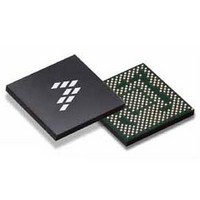
SC900841JVKR2 Freescale Semiconductor, SC900841JVKR2 Datasheet - Page 162

SC900841JVKR2
Manufacturer Part Number
SC900841JVKR2
Description
IC POWER MGT 338-MAPBGA
Manufacturer
Freescale Semiconductor
Specifications of SC900841JVKR2
Applications
PC's, PDA's
Operating Temperature
-40°C ~ 85°C
Mounting Type
Surface Mount
Package / Case
338-TBGA
Input Voltage
2.8 V to 4.4 V
Maximum Operating Temperature
+ 85 C
Minimum Operating Temperature
- 40 C
Lead Free Status / RoHS Status
Lead free / RoHS Compliant
Current - Supply
-
Voltage - Supply
-
Lead Free Status / Rohs Status
Lead free / RoHS Compliant
Available stocks
Company
Part Number
Manufacturer
Quantity
Price
Company:
Part Number:
SC900841JVKR2
Manufacturer:
Freescale Semiconductor
Quantity:
10 000
- Current page: 162 of 192
- Download datasheet (8Mb)
Table 106. Charger Current Reading Coding
Table 105. Application Supply Voltage Reading Coding
CHARGER CURRENT (IF USED)
monitoring the voltage drop over the charge current sense
resistor. This can be enabled by setting the CHRGICON bit in
the FSLADCCNTL register to 1. This resistor is connected
between the ISNSBATP and ISNSBATN pins. The voltage
difference is first amplified to fit the ADC input range as
V(VISNSBATP-VISNSBATN)*4. The conversion is read out in
a 2’s complement format, see
corresponds to the current flow from charger to battery, the
negative reading to the current flowing into the charger
terminal.
accuracy of the result as well as the available conversion
range, but also the charge current levels. It is therefore advised
not to select another value other than those suggested in the
ADC section of
BACKUP VOLTAGE (IF USED)
connected to the COINCELL. This is enabled by setting the
162
900841
FUNCTIONAL DEVICE OPERATION
ADC SUBSYSTEM
CONVERSION
0 111 111 111
0 000 000 001
0 000 000 000
1 111 111 111
1 000 000 000
Conversion Code
Channel 24 can be used to read the charge current by
The value of the sense resistor used determines not only the
Channel 25 can be used to read the voltage of the coin cell
1 111 111 111
1 000 010 100
0 000 000 000
CODE
Table
VOLTAGE
-2.346 mV
-1200 mV
2.346 mV
0.000 mV
1200 mV
AT ADC
INPUT
Voltage at ADC input
3.
-300.000 mV
300.000 mV
2.400 V
1.250 V
0.000 V
-0.600 mV
0.600 mV
0.000 mV
V
Table
ISNSBAT
V
BAT
-
106. The positive reading
THROUGH
CURRENT
0.0059 A
0.0059 A
3.000 A
0.000 A
3.000 A
20 M
Voltage at VPWR
4.800 V
2.500 V
0.000 V
Application/
Application/
To Charger
Connection
To Charger
Connection
CURRENT
Battery
Battery
FLOW
To
To
-
LICON bit in the FSLADCCNTL register to 1. Since the voltage
range of the coin cell exceeds the input voltage range of the
ADC, the COINCELL voltage is first scaled as V
BATTERY DETECT (IF USED)
removal has to be detected to avoid fraudulent use of the
phone. An easy way of doing so is to place the SIM card holder
under the battery pack and perform a battery thermistor
presence check. When the thermistor terminal becomes high-
impedance, the battery is considered being removed. This
detection function can be available at Channel 26 of the ADC
by setting the BATDETVCON bit in the FSLADCCNTL register
to 1. When not charging, the SIM removal function is not
required to operate. Although the additional current drain due
to the battery detect function is small, it is advised to disable the
function when not charging to save this current.
TOUCH SCREEN INTERFACE
channels with built in bias control. The BIAS FET control bits
are part of the ADC round robin address register ADCADDRx.
The touch screen X plate is connected to ADIN10 (X+) and
ADIN11 (X-), while the Y plate is connected to ADIN12(Y+) and
ADIN13(Y-). A local supply, TSREF, of 1.2 V will serve as a
reference.
sequencing and any necessary conversion delays. The system
processor will direct the desired bias control for every reading
though the ADCADDRx registers. If FET biasing is enabled
though the ADCADDRx registers, then touch screen readings
will start according based on the channels chosen, and also by
the ADCADDRx registers. If the touch screen is not used, then
the above inputs can be used as general purpose inputs. In this
case, the bias control will always be programmed to no bias.
Table 107. Backup (Coin Cell) Voltage Reading Coding
Conversion Code Voltage at ADC input Voltage at COINCELL
When a phone is on and supplied by the charger, SIM
The PMIC touch screen support consists of four analog input
The system processor will handle the touch screen
Figure 76
1 111 111 111
1 000 000 000
0 000 000 000
is a touch screen representation.
Analog Integrated Circuit Device Data
2.400 V
1.200 V
0.000 V
Freescale Semiconductor
3.600 V
1.800 V
0.000 V
COIN
*2/3.
Related parts for SC900841JVKR2
Image
Part Number
Description
Manufacturer
Datasheet
Request
R
Part Number:
Description:
Ultra-mobile Platform Pmic
Manufacturer:
Freescale Semiconductor, Inc
Datasheet:

Part Number:
Description:
Sc900 Programmable Penta Uldo With Reset And I2c Interface
Manufacturer:
Semtech Corporation
Datasheet:
Part Number:
Description:
Manufacturer:
Freescale Semiconductor, Inc
Datasheet:
Part Number:
Description:
Manufacturer:
Freescale Semiconductor, Inc
Datasheet:
Part Number:
Description:
Manufacturer:
Freescale Semiconductor, Inc
Datasheet:
Part Number:
Description:
Manufacturer:
Freescale Semiconductor, Inc
Datasheet:
Part Number:
Description:
Manufacturer:
Freescale Semiconductor, Inc
Datasheet:
Part Number:
Description:
Manufacturer:
Freescale Semiconductor, Inc
Datasheet:
Part Number:
Description:
Manufacturer:
Freescale Semiconductor, Inc
Datasheet:
Part Number:
Description:
Manufacturer:
Freescale Semiconductor, Inc
Datasheet:
Part Number:
Description:
Manufacturer:
Freescale Semiconductor, Inc
Datasheet:
Part Number:
Description:
Manufacturer:
Freescale Semiconductor, Inc
Datasheet:
Part Number:
Description:
Manufacturer:
Freescale Semiconductor, Inc
Datasheet:
Part Number:
Description:
Manufacturer:
Freescale Semiconductor, Inc
Datasheet:
Part Number:
Description:
Manufacturer:
Freescale Semiconductor, Inc
Datasheet:


