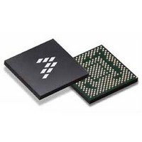
SC900841JVKR2 Freescale Semiconductor, SC900841JVKR2 Datasheet - Page 127

SC900841JVKR2
Manufacturer Part Number
SC900841JVKR2
Description
IC POWER MGT 338-MAPBGA
Manufacturer
Freescale Semiconductor
Specifications of SC900841JVKR2
Applications
PC's, PDA's
Operating Temperature
-40°C ~ 85°C
Mounting Type
Surface Mount
Package / Case
338-TBGA
Input Voltage
2.8 V to 4.4 V
Maximum Operating Temperature
+ 85 C
Minimum Operating Temperature
- 40 C
Lead Free Status / RoHS Status
Lead free / RoHS Compliant
Current - Supply
-
Voltage - Supply
-
Lead Free Status / Rohs Status
Lead free / RoHS Compliant
Available stocks
Company
Part Number
Manufacturer
Quantity
Price
Company:
Part Number:
SC900841JVKR2
Manufacturer:
Freescale Semiconductor
Quantity:
10 000
- Current page: 127 of 192
- Download datasheet (8Mb)
and the temperature range is set at 0°C to 45°C. NTC
circuitry cannot be disabled during charging.
block off through the TEMPEN bit. Whenever an NTC ADC
reading is desired or to keep battery temperature monitor on,
this bit must be asserted. Turning this block off and
disconnecting the switch saves on quiescent current and
enhances battery life. During discharging, the battery
temperature monitoring range is set at -10°C to 60°C.
voltage. The battery thermistor check circuit compares the
fraction of V
COIN CELL BATTERY BACKUP/
CHARGER
backup battery or supercap. If the main battery is deeply
discharged or removed, and in the absence of a USB/Wall
input source, the RTC system and coin cell maintained logic,
will switch over to the COIN CELL for backup power. A small
capacitor should be placed from the COIN CELL pin to
ground under all circumstances.
limited voltage source, resulting in the CC/CV taper
characteristic, typically used for rechargeable Lithium-Ion
batteries. The coin cell charger is enabled via the
COINCHGEN bit. which is enabled by default. The output
Analog Integrated Circuit Device Data
Freescale Semiconductor
During discharging, the user has an option to turn the NTC
The window thresholds are specified as a ratio of the V
The COIN CELL pin provides a connection for a coin cell
The coin cell charger circuit will function as a current
NTC
at NTC pin, with two preset thresholds which
Overtemp
Undertemp
Figure 65. NTC Thermistor Interface
NTC
V
V
HOT
COLD
correspond to one of the previous ranges, depending if the IC
is charging or discharging the battery.
range, charging is stopped and the TEMP interrupt signal is
asserted, to indicate a battery temperature fault. During
discharging if the battery temperature is not within range, the
TEMP interrupt signal is asserted.
well as the comparator offset error. Other applications may
not require an NTC interface. In that case, the NTC resistor is
not populated and this feature is disabled.
voltage (V
bits. The coin cell charger voltage is programmable in the
active state, where the charge current is fixed at I
coin cell charging will be stopped when V
V
a more detailed description of the coin cell related bits.
used instead of a lithium based coin cell. To avoid discharge
by leakage currents from external components or by the
900841, the COINCHGEN bit should always remain set.
that isolates the coin cell from any loads, if V
2.0 V, to prevent the coin cell from being deeply discharged
and damaged. This will also cause the ADC reading of the
coin cell voltage to yield zero.
PWRUVF
During charging, if the battery temperature is not within
The tolerance should include the resistive divider error, as
A large capacitor, electrolytic or super cap, can also be
Coin cell charge is equipped with a disconnect circuitry
V
BATTERY INTERFACE AND POWER PATH MANAGEMENT
CORE
. Reference
COIN
) is programmable through the VCOIN[2:0]
VNTC
NTC
Power Path Manager SPI Registers
R
FUNCTIONAL DEVICE OPERATION
NTC
NTC
PWR
COIN
goes below
COINHI
goes below
900841
. The
127
for
Related parts for SC900841JVKR2
Image
Part Number
Description
Manufacturer
Datasheet
Request
R
Part Number:
Description:
Ultra-mobile Platform Pmic
Manufacturer:
Freescale Semiconductor, Inc
Datasheet:

Part Number:
Description:
Sc900 Programmable Penta Uldo With Reset And I2c Interface
Manufacturer:
Semtech Corporation
Datasheet:
Part Number:
Description:
Manufacturer:
Freescale Semiconductor, Inc
Datasheet:
Part Number:
Description:
Manufacturer:
Freescale Semiconductor, Inc
Datasheet:
Part Number:
Description:
Manufacturer:
Freescale Semiconductor, Inc
Datasheet:
Part Number:
Description:
Manufacturer:
Freescale Semiconductor, Inc
Datasheet:
Part Number:
Description:
Manufacturer:
Freescale Semiconductor, Inc
Datasheet:
Part Number:
Description:
Manufacturer:
Freescale Semiconductor, Inc
Datasheet:
Part Number:
Description:
Manufacturer:
Freescale Semiconductor, Inc
Datasheet:
Part Number:
Description:
Manufacturer:
Freescale Semiconductor, Inc
Datasheet:
Part Number:
Description:
Manufacturer:
Freescale Semiconductor, Inc
Datasheet:
Part Number:
Description:
Manufacturer:
Freescale Semiconductor, Inc
Datasheet:
Part Number:
Description:
Manufacturer:
Freescale Semiconductor, Inc
Datasheet:
Part Number:
Description:
Manufacturer:
Freescale Semiconductor, Inc
Datasheet:
Part Number:
Description:
Manufacturer:
Freescale Semiconductor, Inc
Datasheet:


