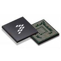
SC900841JVKR2 Freescale Semiconductor, SC900841JVKR2 Datasheet - Page 84

SC900841JVKR2
Manufacturer Part Number
SC900841JVKR2
Description
IC POWER MGT 338-MAPBGA
Manufacturer
Freescale Semiconductor
Specifications of SC900841JVKR2
Applications
PC's, PDA's
Operating Temperature
-40°C ~ 85°C
Mounting Type
Surface Mount
Package / Case
338-TBGA
Input Voltage
2.8 V to 4.4 V
Maximum Operating Temperature
+ 85 C
Minimum Operating Temperature
- 40 C
Lead Free Status / RoHS Status
Lead free / RoHS Compliant
Current - Supply
-
Voltage - Supply
-
Lead Free Status / Rohs Status
Lead free / RoHS Compliant
Available stocks
Company
Part Number
Manufacturer
Quantity
Price
Company:
Part Number:
SC900841JVKR2
Manufacturer:
Freescale Semiconductor
Quantity:
10 000
- Current page: 84 of 192
- Download datasheet (8Mb)
Main Features
• Supplies signaling/status LEDs and USB OTG
• Uses the V
• Supports up to 350 mA of output current at a 5.0 V fixed
• 2.0 MHz switching frequency
• Uses internal compensation
• Soft start feature to minimize inrush currents at power up
• Uses an internal low side switch MOSFET
.
VOTG Status/Control Registers and Bits Description
to provide extended functionality to the VOTG regulator.
84
Table 40. VOTG Status and Control Registers Structure and Bits Description
900841
FUNCTIONAL DEVICE OPERATION
POWER SUPPLIES
AOACCTLVOTG
output voltage
The following registers are defined by Freescale in order
CTLVOTG
Reserved
Name
PWR
rail as its power supply
Bits
2:0
5:3
7:6
VOTG State Control
x0 = Reserved
x1 = Reserved
x2 = Reserved
x3 = Reserved
VOTG State Control during AOAC Exit (when the Exit pin is EXITSTBY pin is asserted). These bits will be initialized
by the system SPI controller after power up.
X0 = Don’t Copy
x1 = Don’t Copy
x2 = Don’t Copy
x3 = Don’t Copy
Reserved
FSLVOTGCNTL2 (ADDR 0x1C6 - R/W - Default Value: 0x24)
Figure 39. VOTG Efficiency Curves
• Gate drive circuits are supplied directly from V
• Output over-voltage, over-current, and short-circuit
• External switch control for output isolation when needed
Efficiency Curves
the recommended external component values and typical
output voltage. 3.0 V ≤ VPWR ≤ 4.4 V. The following curves
do not take in account the switch drop across M
protection
The following efficiency curves are calculated, based on
Description
x4 = VOTG is OFF
x5 = Not Used
x6 = Not Used
x7 = VOTG is ON
x4 = VOTG is OFF
x5 = Not Used
x6 = Not Used
x7 = VOTG is ON
Analog Integrated Circuit Device Data
Freescale Semiconductor
OTG.
PWR
Related parts for SC900841JVKR2
Image
Part Number
Description
Manufacturer
Datasheet
Request
R
Part Number:
Description:
Ultra-mobile Platform Pmic
Manufacturer:
Freescale Semiconductor, Inc
Datasheet:

Part Number:
Description:
Sc900 Programmable Penta Uldo With Reset And I2c Interface
Manufacturer:
Semtech Corporation
Datasheet:
Part Number:
Description:
Manufacturer:
Freescale Semiconductor, Inc
Datasheet:
Part Number:
Description:
Manufacturer:
Freescale Semiconductor, Inc
Datasheet:
Part Number:
Description:
Manufacturer:
Freescale Semiconductor, Inc
Datasheet:
Part Number:
Description:
Manufacturer:
Freescale Semiconductor, Inc
Datasheet:
Part Number:
Description:
Manufacturer:
Freescale Semiconductor, Inc
Datasheet:
Part Number:
Description:
Manufacturer:
Freescale Semiconductor, Inc
Datasheet:
Part Number:
Description:
Manufacturer:
Freescale Semiconductor, Inc
Datasheet:
Part Number:
Description:
Manufacturer:
Freescale Semiconductor, Inc
Datasheet:
Part Number:
Description:
Manufacturer:
Freescale Semiconductor, Inc
Datasheet:
Part Number:
Description:
Manufacturer:
Freescale Semiconductor, Inc
Datasheet:
Part Number:
Description:
Manufacturer:
Freescale Semiconductor, Inc
Datasheet:
Part Number:
Description:
Manufacturer:
Freescale Semiconductor, Inc
Datasheet:
Part Number:
Description:
Manufacturer:
Freescale Semiconductor, Inc
Datasheet:


