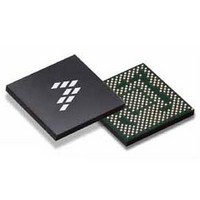
SC900841JVKR2 Freescale Semiconductor, SC900841JVKR2 Datasheet - Page 43

SC900841JVKR2
Manufacturer Part Number
SC900841JVKR2
Description
IC POWER MGT 338-MAPBGA
Manufacturer
Freescale Semiconductor
Specifications of SC900841JVKR2
Applications
PC's, PDA's
Operating Temperature
-40°C ~ 85°C
Mounting Type
Surface Mount
Package / Case
338-TBGA
Input Voltage
2.8 V to 4.4 V
Maximum Operating Temperature
+ 85 C
Minimum Operating Temperature
- 40 C
Lead Free Status / RoHS Status
Lead free / RoHS Compliant
Current - Supply
-
Voltage - Supply
-
Lead Free Status / Rohs Status
Lead free / RoHS Compliant
Available stocks
Company
Part Number
Manufacturer
Quantity
Price
Company:
Part Number:
SC900841JVKR2
Manufacturer:
Freescale Semiconductor
Quantity:
10 000
- Current page: 43 of 192
- Download datasheet (8Mb)
• Next five bits, SDATA[15:11] are dedicated to core voltage
• Following five bits, SDATA[10:6] are reserved
• Last six bits, SDATA[5:0] are unused. These bits are read
• Changes to core supply voltage levels are applied only
through 15 as follows:
INTERRUPT CONTROLLER
Control
interrupts. Unmasked interrupt events are signaled to the
host by driving the PMICINT pin high.
becomes inactive, the interrupt will remain set until cleared. If
a new interrupt occurs while the controller clears an existing
interrupt bit, the interrupt line will remain high.
corresponding mask bit to a ‘1’. As a result, when a masked
interrupt bit goes high, the interrupt line will not go high. A
masked interrupt can still be read from the register. If a
masked interrupt bit was already high, the interrupt line will go
high after unmasking.
has inherent latency that the clients must expect:
Analog Integrated Circuit Device Data
Freescale Semiconductor
1. PMIC interrupts SCU, if both the 1st and 2nd level bits
2. SCU reads PMIC master, 1st level, interrupt event
it is ready to receive the next word. This improves the
noise immunity of the system.
levels
as zeroes
after receiving all 16-bits of data
The VYMX3G output voltage is determined by bits 11
The PMIC informs the system of important events using
Each interrupt is latched so that even if the interrupt source
Each interrupt can be masked by setting the
The following is the interrupt handling mechanism which
are not masked.
register.
Figure 8. Mini-SPI Architecture and Simplified Timing Diagram
SC900841
Table 9. Advanced COMMs Mini-SPI Pin Functionality
• VYMX3G =0.6V+ 0.025*{2^4*SDATA[15] +
• The 2nd level bit is set.
• The 1st level bit is set by a rising edge sent from the 2nd
• When the system controller, the SCU, reads the 1st level
• When the 1st level register is read, any 1st level register
3. SCU then traverses all the branches of the interrupt
4. SCU will service events in leaf node registers.
2^3*SDATA[14] + 2^2*SDATA[13] + 2^1*SDATA[12] +
SDATA[11]}
When an unmasked interrupt event happens:
level register, and the PMICINT signal goes from low to
high
register the 2nd level registers that were set, remain set.
Any unset registers are free to accept an interrupt event.
bits that were set at the point the SPI read strobe shifts the
register value into the SPI transmit shift register, that bit
will be cleared by the SPI self clear signal immediately
following the read strobe. This allows new interrupts to be
recorded without being lost. If all unmasked 1st level bits
get cleared by the read, the PIMCINT pin will de-assert. If
a new unmasked 1st level interrupt event happens, just
after the read of the 1st level register, the PIMCINT pin
interrupt pin will remain asserted. The SCU reads each
2nd level register and these are cleared on read.
Pin Name
tree where events are indicated.
SDATA
SCK
CS
Advanced COMMs SPI Bus Data In
Advanced COMMs SPI Bus Clock Input
Advanced COMMs SPI Bus Chip Select Input
FUNCTIONAL DEVICE OPERATION
SYSTEM CONTROL INTERFACE
Pin Functionality
900841
43
Related parts for SC900841JVKR2
Image
Part Number
Description
Manufacturer
Datasheet
Request
R
Part Number:
Description:
Ultra-mobile Platform Pmic
Manufacturer:
Freescale Semiconductor, Inc
Datasheet:

Part Number:
Description:
Sc900 Programmable Penta Uldo With Reset And I2c Interface
Manufacturer:
Semtech Corporation
Datasheet:
Part Number:
Description:
Manufacturer:
Freescale Semiconductor, Inc
Datasheet:
Part Number:
Description:
Manufacturer:
Freescale Semiconductor, Inc
Datasheet:
Part Number:
Description:
Manufacturer:
Freescale Semiconductor, Inc
Datasheet:
Part Number:
Description:
Manufacturer:
Freescale Semiconductor, Inc
Datasheet:
Part Number:
Description:
Manufacturer:
Freescale Semiconductor, Inc
Datasheet:
Part Number:
Description:
Manufacturer:
Freescale Semiconductor, Inc
Datasheet:
Part Number:
Description:
Manufacturer:
Freescale Semiconductor, Inc
Datasheet:
Part Number:
Description:
Manufacturer:
Freescale Semiconductor, Inc
Datasheet:
Part Number:
Description:
Manufacturer:
Freescale Semiconductor, Inc
Datasheet:
Part Number:
Description:
Manufacturer:
Freescale Semiconductor, Inc
Datasheet:
Part Number:
Description:
Manufacturer:
Freescale Semiconductor, Inc
Datasheet:
Part Number:
Description:
Manufacturer:
Freescale Semiconductor, Inc
Datasheet:
Part Number:
Description:
Manufacturer:
Freescale Semiconductor, Inc
Datasheet:


