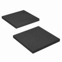
EP4SGX290KF40C3N Altera, EP4SGX290KF40C3N Datasheet - Page 143

EP4SGX290KF40C3N
Manufacturer Part Number
EP4SGX290KF40C3N
Description
IC STRATIX IV GX 290K 1517FBGA
Manufacturer
Altera
Series
Stratix® IV GXr
Datasheets
1.EP4SGX110DF29C3N.pdf
(80 pages)
2.EP4SGX110DF29C3N.pdf
(1154 pages)
3.EP4SGX110DF29C3N.pdf
(432 pages)
4.EP4SGX110DF29C3N.pdf
(22 pages)
5.EP4SGX110DF29C3N.pdf
(30 pages)
6.EP4SGX110DF29C3N.pdf
(72 pages)
Specifications of EP4SGX290KF40C3N
Number Of Logic Elements/cells
291200
Number Of Labs/clbs
11648
Total Ram Bits
17248
Number Of I /o
744
Voltage - Supply
0.87 V ~ 0.93 V
Mounting Type
Surface Mount
Operating Temperature
0°C ~ 85°C
Package / Case
1517-FBGA
Lead Free Status / RoHS Status
Lead free / RoHS Compliant
Number Of Gates
-
Other names
544-2624
Available stocks
Company
Part Number
Manufacturer
Quantity
Price
- EP4SGX110DF29C3N PDF datasheet
- EP4SGX110DF29C3N PDF datasheet #2
- EP4SGX110DF29C3N PDF datasheet #3
- EP4SGX110DF29C3N PDF datasheet #4
- EP4SGX110DF29C3N PDF datasheet #5
- EP4SGX110DF29C3N PDF datasheet #6
- Current page: 143 of 1154
- Download datasheet (32Mb)
Chapter 5: Clock Networks and PLLs in Stratix IV Devices
PLLs in Stratix IV Devices
February 2011 Altera Corporation
Clock Feedback Modes
1
Stratix IV PLLs support up to six different clock feedback modes. Each mode allows
clock multiplication and division, phase shifting, and programmable duty cycle.
Table 5–9
Table 5–9. Clock Feedback Mode Availability
The input and output delays are fully compensated by a PLL only when using the
dedicated clock input pins associated with a given PLL as the clock source. For
example, when using PLL_T1 in normal mode, the clock delays from the input pin to
the PLL clock output-to-destination register are fully compensated, provided the
clock input pin is one of the following two pins: CLK14 and CLK15. Compensated pins
are only in the same I/O bank as the PLL. When an RCLK or GCLK network drives
the PLL, the input and output delays may not be fully compensated in the Quartus II
software. Another example is when you configure PLL_T2 in zero-delay buffer mode
and the PLL input is driven by a dedicated clock input pin, a fully compensated clock
path results in zero-delay between the clock input and one of the output clocks from
the PLL. If the PLL input is instead fed by a non-dedicated input (using the GCLK
network), the output clock may not be perfectly aligned with the input clock.
Source-synchronous
No-compensation
Normal
Zero-delay buffer (ZDB)
External feedback
LVDS compensation
Notes to
(1) The high-bandwidth PLL setting is not supported in external feedback mode.
(2) External feedback mode is supported for single-ended inputs and outputs only on the left and right PLLs.
Table
Clock Feedback Mode
lists the clock feedback modes supported by the Stratix IV device PLLs.
5–9:
(1)
Top and Bottom PLLs
Yes
Yes
Yes
Yes
Yes
No
Availability
Stratix IV Device Handbook Volume 1
Left and Right PLLs
Yes
Yes
Yes
Yes
Yes
Yes
(2)
5–27
Related parts for EP4SGX290KF40C3N
Image
Part Number
Description
Manufacturer
Datasheet
Request
R

Part Number:
Description:
CYCLONE II STARTER KIT EP2C20N
Manufacturer:
Altera
Datasheet:

Part Number:
Description:
CPLD, EP610 Family, ECMOS Process, 300 Gates, 16 Macro Cells, 16 Reg., 16 User I/Os, 5V Supply, 35 Speed Grade, 24DIP
Manufacturer:
Altera Corporation
Datasheet:

Part Number:
Description:
CPLD, EP610 Family, ECMOS Process, 300 Gates, 16 Macro Cells, 16 Reg., 16 User I/Os, 5V Supply, 15 Speed Grade, 24DIP
Manufacturer:
Altera Corporation
Datasheet:

Part Number:
Description:
Manufacturer:
Altera Corporation
Datasheet:

Part Number:
Description:
CPLD, EP610 Family, ECMOS Process, 300 Gates, 16 Macro Cells, 16 Reg., 16 User I/Os, 5V Supply, 30 Speed Grade, 24DIP
Manufacturer:
Altera Corporation
Datasheet:

Part Number:
Description:
High-performance, low-power erasable programmable logic devices with 8 macrocells, 10ns
Manufacturer:
Altera Corporation
Datasheet:

Part Number:
Description:
High-performance, low-power erasable programmable logic devices with 8 macrocells, 7ns
Manufacturer:
Altera Corporation
Datasheet:

Part Number:
Description:
Classic EPLD
Manufacturer:
Altera Corporation
Datasheet:

Part Number:
Description:
High-performance, low-power erasable programmable logic devices with 8 macrocells, 10ns
Manufacturer:
Altera Corporation
Datasheet:

Part Number:
Description:
Manufacturer:
Altera Corporation
Datasheet:

Part Number:
Description:
Manufacturer:
Altera Corporation
Datasheet:

Part Number:
Description:
Manufacturer:
Altera Corporation
Datasheet:

Part Number:
Description:
CPLD, EP610 Family, ECMOS Process, 300 Gates, 16 Macro Cells, 16 Reg., 16 User I/Os, 5V Supply, 25 Speed Grade, 24DIP
Manufacturer:
Altera Corporation
Datasheet:


