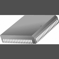
MC68EC000EI8 Freescale Semiconductor, MC68EC000EI8 Datasheet - Page 172

MC68EC000EI8
Manufacturer Part Number
MC68EC000EI8
Description
IC MPU 32BIT 85MHZ 68-PLCC
Manufacturer
Freescale Semiconductor
Series
M68000r
Specifications of MC68EC000EI8
Processor Type
M680x0 32-Bit
Speed
8MHz
Voltage
3.3V, 5V
Mounting Type
Surface Mount
Package / Case
68-PLCC
Core Size
32 Bit
Cpu Speed
8MHz
Digital Ic Case Style
PLCC
No. Of Pins
68
Supply Voltage Range
3V To 3.6V
Operating Temperature Range
0°C To +70°C
Filter Terminals
SMD
Rohs Compliant
Yes
Clock Frequency
8MHz
Lead Free Status / RoHS Status
Lead free / RoHS Compliant
Features
-
Available stocks
Company
Part Number
Manufacturer
Quantity
Price
Company:
Part Number:
MC68EC000EI8
Manufacturer:
XILINX
Quantity:
661
Company:
Part Number:
MC68EC000EI8
Manufacturer:
Freescale Semiconductor
Quantity:
10 000
Company:
Part Number:
MC68EC000EI8R2
Manufacturer:
Freescale Semiconductor
Quantity:
10 000
- Current page: 172 of 646
- Download datasheet (3Mb)
Integer Instructions
CAS
CAS2
Instruction Format:
Instruction Fields:
4-68
D/A1
D/A2
15
0
Size field—Specifies the size of the operation.
D/A1, D/A2 fields—Specify whether Rn1 and Rn2 reference data or address registers,
Rn1, Rn2 fields—Specify the numbers of the registers that contain the addresses of
Du1, Du2 fields—Specify the data registers that contain the update values to be written
Dc1, Dc2 fields—Specify the data registers that contain the test values to be compared
10 — Word operation
11 — Long operation
0 — The corresponding register is a data register.
1 — The corresponding register is an address register.
14
0
respectively.
the first and second memory operands, respectively. If the operands overlap in
memory, the results of any memory update are undefined.
to the first and second memory operand locations if the comparison is successful.
to the first and second memory operands, respectively. If Dc1 and Dc2 specify the
same data register and the comparison fails, memory operand 1 is stored in the
data register.
Rn1
Rn2
13
The CAS and CAS2 instructions can be used to perform secure
update operations on system control data structures in a
multiprocessing environment.
In the MC68040 if the operands are not equal, the destination or
destination 1 operand is written back to memory to complete the
locked access for CAS or CAS2, respectively.
0
12
0
M68000 FAMILY PROGRAMMER’S REFERENCE MANUAL
Compare and Swap with Operand
11
1
0
0
(MC68020, MC68030, MC68040)
10
0
0
SIZE
9
0
0
8
0
NOTE
CAS2
Du1
Du2
7
1
6
1
5
1
0
0
4
1
0
0
3
1
0
0
2
1
CAS2
MOTOROLA
Dc1
Dc2
CAS
1
0
0
0
Related parts for MC68EC000EI8
Image
Part Number
Description
Manufacturer
Datasheet
Request
R
Part Number:
Description:
Manufacturer:
Freescale Semiconductor, Inc
Datasheet:
Part Number:
Description:
Manufacturer:
Freescale Semiconductor, Inc
Datasheet:
Part Number:
Description:
Manufacturer:
Freescale Semiconductor, Inc
Datasheet:
Part Number:
Description:
Manufacturer:
Freescale Semiconductor, Inc
Datasheet:
Part Number:
Description:
Manufacturer:
Freescale Semiconductor, Inc
Datasheet:
Part Number:
Description:
Manufacturer:
Freescale Semiconductor, Inc
Datasheet:
Part Number:
Description:
Manufacturer:
Freescale Semiconductor, Inc
Datasheet:
Part Number:
Description:
Manufacturer:
Freescale Semiconductor, Inc
Datasheet:
Part Number:
Description:
Manufacturer:
Freescale Semiconductor, Inc
Datasheet:
Part Number:
Description:
Manufacturer:
Freescale Semiconductor, Inc
Datasheet:
Part Number:
Description:
Manufacturer:
Freescale Semiconductor, Inc
Datasheet:
Part Number:
Description:
Manufacturer:
Freescale Semiconductor, Inc
Datasheet:
Part Number:
Description:
Manufacturer:
Freescale Semiconductor, Inc
Datasheet:
Part Number:
Description:
Manufacturer:
Freescale Semiconductor, Inc
Datasheet:
Part Number:
Description:
Manufacturer:
Freescale Semiconductor, Inc
Datasheet:


