M68EVB908GB60E Freescale Semiconductor, M68EVB908GB60E Datasheet - Page 118
M68EVB908GB60E
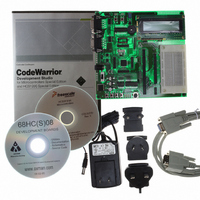
Manufacturer Part Number
M68EVB908GB60E
Description
BOARD EVAL FOR MC9S08GB60
Manufacturer
Freescale Semiconductor
Type
MCUr
Datasheet
1.M68EVB908GB60E.pdf
(290 pages)
Specifications of M68EVB908GB60E
Contents
Module and Misc Hardware
Processor To Be Evaluated
MC9S08GB
Data Bus Width
8 bit
Interface Type
RS-232
Silicon Manufacturer
Freescale
Core Architecture
HCS08
Core Sub-architecture
HCS08
Silicon Core Number
MC9S08
Silicon Family Name
S08GB
Kit Contents
GB60 Evaluation Kit
Rohs Compliant
Yes
For Use With/related Products
MC9S08GB60
Lead Free Status / RoHS Status
Lead free / RoHS Compliant


Internal Clock Generator (ICG) Module
7.5.1
RANGE — Frequency Range Select
REFS — External Reference Select
CLKS — Clock Mode Select
The CLKS bits are writable at any time, unless the first write after a reset was CLKS = 0X, the CLKS bits
cannot be written to 1X until after the next reset (because the EXTAL pin was not reserved).
118
1. This bit is reserved for Freescale Semiconductor internal use only. Any write operations to this register should write
The RANGE bit controls the oscillator, reference divider, and FLL loop prescaler multiplication factor
(P). It selects one of two reference frequency ranges for the ICG. The RANGE bit is write-once after
a reset. The RANGE bit only has an effect in FLL engaged external and FLL bypassed external modes.
The REFS bit controls the external reference clock source for ICGERCLK. The REFS bit is write-once
after a reset.
The CLKS bits control the clock mode according to
requested, it will not be selected until ERCS = 1. If the ICG enters off mode, the CLKS bits will remain
unchanged.Writes to the CLKS bits will not take effect if a previous write is not complete.
a 0 to this bit.
1 = Oscillator configured for high frequency range. FLL loop prescale factor P is 1.
0 = Oscillator configured for low frequency range. FLL loop prescale factor P is 64.
1 = Oscillator using crystal or resonator requested.
0 = External clock requested.
ICG Control Register 1 (ICGC1)
Reset:
Read:
Write:
Bit 7
0
0
CLKS[1:0]
Figure 7-12. ICG Control Register 1 (ICGC1)
00
01
10
11
= Unimplemented or Reserved
RANGE
MC9S08GB/GT Data Sheet, Rev. 2.3
Figure 7-13. CLKS Clock Select
6
1
REFS
FLL bypassed, external reference
FLL engaged, external reference
FLL engaged, internal reference
5
0
Self-clocked
Clock Mode
Figure
4
0
CLKS
7-13. If FLL bypassed external is
3
0
OSCSTEN
2
1
Freescale Semiconductor
0
1
(1)
0
Bit 0
0
0
Related parts for M68EVB908GB60E
Image
Part Number
Description
Manufacturer
Datasheet
Request
R

Part Number:
Description:
Manufacturer:
Freescale Semiconductor, Inc
Datasheet:
Part Number:
Description:
Manufacturer:
Freescale Semiconductor, Inc
Datasheet:
Part Number:
Description:
Manufacturer:
Freescale Semiconductor, Inc
Datasheet:
Part Number:
Description:
Manufacturer:
Freescale Semiconductor, Inc
Datasheet:
Part Number:
Description:
Manufacturer:
Freescale Semiconductor, Inc
Datasheet:
Part Number:
Description:
Manufacturer:
Freescale Semiconductor, Inc
Datasheet:
Part Number:
Description:
Manufacturer:
Freescale Semiconductor, Inc
Datasheet:
Part Number:
Description:
Manufacturer:
Freescale Semiconductor, Inc
Datasheet:
Part Number:
Description:
Manufacturer:
Freescale Semiconductor, Inc
Datasheet:
Part Number:
Description:
Manufacturer:
Freescale Semiconductor, Inc
Datasheet:
Part Number:
Description:
Manufacturer:
Freescale Semiconductor, Inc
Datasheet:
Part Number:
Description:
Manufacturer:
Freescale Semiconductor, Inc
Datasheet:
Part Number:
Description:
Manufacturer:
Freescale Semiconductor, Inc
Datasheet:
Part Number:
Description:
Manufacturer:
Freescale Semiconductor, Inc
Datasheet:
Part Number:
Description:
Manufacturer:
Freescale Semiconductor, Inc
Datasheet: