M68EVB908GB60E Freescale Semiconductor, M68EVB908GB60E Datasheet - Page 223
M68EVB908GB60E
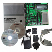
Manufacturer Part Number
M68EVB908GB60E
Description
BOARD EVAL FOR MC9S08GB60
Manufacturer
Freescale Semiconductor
Type
MCUr
Datasheet
1.M68EVB908GB60E.pdf
(290 pages)
Specifications of M68EVB908GB60E
Contents
Module and Misc Hardware
Processor To Be Evaluated
MC9S08GB
Data Bus Width
8 bit
Interface Type
RS-232
Silicon Manufacturer
Freescale
Core Architecture
HCS08
Core Sub-architecture
HCS08
Silicon Core Number
MC9S08
Silicon Family Name
S08GB
Kit Contents
GB60 Evaluation Kit
Rohs Compliant
Yes
For Use With/related Products
MC9S08GB60
Lead Free Status / RoHS Status
Lead free / RoHS Compliant


14.2.1.1 Channel Input Pins — AD1P7–AD1P0
The channel pins are used as the analog input pins of the ATD. Each pin is connected to an analog switch
which serves as the signal gate into the sample submodule.
14.2.1.2 ATD Reference Pins — V
These pins serve as the source for the high and low reference potentials for the converter. Separation from
the power supply pins accommodates the filtering necessary to achieve the accuracy of which the system
is capable.
14.2.1.3 ATD Supply Pins — V
These two pins are used to supply power and ground to the analog section of the ATD. Dedicated power
is required to isolate the sensitive analog circuitry from the normal levels of noise present on digital power
supplies.
14.3
The ATD uses a successive approximation register (SAR) architecture. The ATD contains all the necessary
elements to perform a single analog-to-digital conversion.
A write to the ATD1SC register initiates a new conversion. A write to the ATD1C register will interrupt
the current conversion but it will not initiate a new conversion. A write to the ATD1PE register will also
abort the current conversion but will not initiate a new conversion. If a conversion is already running when
a write to the ATD1SC register is made, it will be aborted and a new one will be started.
14.3.1
The ATD has a mode control unit to communicate with the sample and hold (S/H) machine and the SAR
machine when necessary to collect samples and perform conversions. The mode control unit signals the
S/H machine to begin collecting a sample and for the SAR machine to begin receiving a sample. At the
end of the sample period, the S/H machine signals the SAR machine to begin the analog-to-digital
conversion process. The conversion process is terminated when the SAR machine signals the end of
Freescale Semiconductor
Functional Description
Mode Control
V
must be at the same potential.
DDAD1
and V
AD7–AD0
DD
V
V
V
Name
V
DDAD
REFH
SSAD
REFL
must be at the same potential. Likewise, V
MC9S08GB/GT Data Sheet, Rev. 2.3
Table 14-1. Signal Properties
DDAD
High reference voltage for ATD converter
Low reference voltage for ATD converter
REFH
, V
ATD ground supply voltage
ATD power supply voltage
NOTE
SSAD
, V
Channel input pins
REFL
Function
SSAD1
and V
Functional Description
SS
223
Related parts for M68EVB908GB60E
Image
Part Number
Description
Manufacturer
Datasheet
Request
R

Part Number:
Description:
Manufacturer:
Freescale Semiconductor, Inc
Datasheet:
Part Number:
Description:
Manufacturer:
Freescale Semiconductor, Inc
Datasheet:
Part Number:
Description:
Manufacturer:
Freescale Semiconductor, Inc
Datasheet:
Part Number:
Description:
Manufacturer:
Freescale Semiconductor, Inc
Datasheet:
Part Number:
Description:
Manufacturer:
Freescale Semiconductor, Inc
Datasheet:
Part Number:
Description:
Manufacturer:
Freescale Semiconductor, Inc
Datasheet:
Part Number:
Description:
Manufacturer:
Freescale Semiconductor, Inc
Datasheet:
Part Number:
Description:
Manufacturer:
Freescale Semiconductor, Inc
Datasheet:
Part Number:
Description:
Manufacturer:
Freescale Semiconductor, Inc
Datasheet:
Part Number:
Description:
Manufacturer:
Freescale Semiconductor, Inc
Datasheet:
Part Number:
Description:
Manufacturer:
Freescale Semiconductor, Inc
Datasheet:
Part Number:
Description:
Manufacturer:
Freescale Semiconductor, Inc
Datasheet:
Part Number:
Description:
Manufacturer:
Freescale Semiconductor, Inc
Datasheet:
Part Number:
Description:
Manufacturer:
Freescale Semiconductor, Inc
Datasheet:
Part Number:
Description:
Manufacturer:
Freescale Semiconductor, Inc
Datasheet: