M68EVB908GB60E Freescale Semiconductor, M68EVB908GB60E Datasheet - Page 234
M68EVB908GB60E
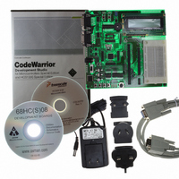
Manufacturer Part Number
M68EVB908GB60E
Description
BOARD EVAL FOR MC9S08GB60
Manufacturer
Freescale Semiconductor
Type
MCUr
Datasheet
1.M68EVB908GB60E.pdf
(290 pages)
Specifications of M68EVB908GB60E
Contents
Module and Misc Hardware
Processor To Be Evaluated
MC9S08GB
Data Bus Width
8 bit
Interface Type
RS-232
Silicon Manufacturer
Freescale
Core Architecture
HCS08
Core Sub-architecture
HCS08
Silicon Core Number
MC9S08
Silicon Family Name
S08GB
Kit Contents
GB60 Evaluation Kit
Rohs Compliant
Yes
For Use With/related Products
MC9S08GB60
Lead Free Status / RoHS Status
Lead free / RoHS Compliant


Analog-to-Digital Converter (ATD) Module
14.6.3
For left-justified mode, result data bits 9–2 map onto bits 7–0 of ATD1RH, result data bits 1 and 0 map
onto ATD1RL bits 7 and 6, where bit 7 of ATD1RH is the most significant bit (MSB).
For right-justified mode, result data bits 9 and 8 map onto bits 1 and 0 of ATD1RH, result data bits 7–0
map onto ATD1RL bits 7–0, where bit 1 of ATD1RH is the most significant bit (MSB).
The ATD 10-bit conversion results are stored in two 8-bit result registers, ATD1RH and ATD1RL. The
result data is formatted either left or right justified where the format is selected using the DJM control bit
in the ATD1C register. The 10-bit result data is mapped either between ATD1RH bits 7–0 and ATD1RL
bits 7–6 (left justified), or ATD1RH bits 1–0 and ATD1RL bits 7–0 (right justified).
For 8-bit conversions, the 8-bit result is always located in ATD1RH bits 7–0, and the ATD1RL bits read 0.
For 10-bit conversions, the six unused bits always read 0.
The ATD1RH and ATD1RL registers are read-only.
14.6.4
The ATD pin enable register allows the pins dedicated to the ATD module to be configured for ATD usage.
A write to this register will abort the current conversion but will not initiate a new conversion. If the
ATDPEx bit is 0 (disabled for ATD usage) but the corresponding analog input channel is selected via the
ATDCH bits, the ATD will not convert the analog input but will instead convert V
the ATD result registers.
ATDPE7:ATDPE0 — ATD Pin 7–0 Enables
234
ATD1RH
ATD1RH
7
9
7
1 = Pin enabled for ATD usage.
0 = Pin disabled for ATD usage.
ATD Result Data (ATD1RH, ATD1RL)
ATD Pin Enable (ATD1PE)
6
6
5
5
Reset:
Read:
Write:
4
4
ATDPE7
Figure 14-11. ATD Pin Enable Register (ATD1PE)
Bit 7
3
3
0
RESULT
Figure 14-10. Right-Justified Mode
2
2
ATDPE6
Figure 14-9. Left-Justified Mode
MC9S08GB/GT Data Sheet, Rev. 2.3
6
0
1
1
9
ATDPE5
0
0
5
0
ATD1RL
ATD1RL
ATDPE4
7
7
4
0
6
0
6
ATDPE3
3
0
RESULT
5
5
ATDPE2
4
4
2
0
3
3
ATDPE1
REFL
Freescale Semiconductor
1
0
2
2
placing zeroes in
ATDPE0
Bit 0
1
1
0
0
0
0
Related parts for M68EVB908GB60E
Image
Part Number
Description
Manufacturer
Datasheet
Request
R

Part Number:
Description:
Manufacturer:
Freescale Semiconductor, Inc
Datasheet:
Part Number:
Description:
Manufacturer:
Freescale Semiconductor, Inc
Datasheet:
Part Number:
Description:
Manufacturer:
Freescale Semiconductor, Inc
Datasheet:
Part Number:
Description:
Manufacturer:
Freescale Semiconductor, Inc
Datasheet:
Part Number:
Description:
Manufacturer:
Freescale Semiconductor, Inc
Datasheet:
Part Number:
Description:
Manufacturer:
Freescale Semiconductor, Inc
Datasheet:
Part Number:
Description:
Manufacturer:
Freescale Semiconductor, Inc
Datasheet:
Part Number:
Description:
Manufacturer:
Freescale Semiconductor, Inc
Datasheet:
Part Number:
Description:
Manufacturer:
Freescale Semiconductor, Inc
Datasheet:
Part Number:
Description:
Manufacturer:
Freescale Semiconductor, Inc
Datasheet:
Part Number:
Description:
Manufacturer:
Freescale Semiconductor, Inc
Datasheet:
Part Number:
Description:
Manufacturer:
Freescale Semiconductor, Inc
Datasheet:
Part Number:
Description:
Manufacturer:
Freescale Semiconductor, Inc
Datasheet:
Part Number:
Description:
Manufacturer:
Freescale Semiconductor, Inc
Datasheet:
Part Number:
Description:
Manufacturer:
Freescale Semiconductor, Inc
Datasheet: