M68EVB908GB60E Freescale Semiconductor, M68EVB908GB60E Datasheet - Page 82
M68EVB908GB60E
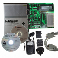
Manufacturer Part Number
M68EVB908GB60E
Description
BOARD EVAL FOR MC9S08GB60
Manufacturer
Freescale Semiconductor
Type
MCUr
Datasheet
1.M68EVB908GB60E.pdf
(290 pages)
Specifications of M68EVB908GB60E
Contents
Module and Misc Hardware
Processor To Be Evaluated
MC9S08GB
Data Bus Width
8 bit
Interface Type
RS-232
Silicon Manufacturer
Freescale
Core Architecture
HCS08
Core Sub-architecture
HCS08
Silicon Core Number
MC9S08
Silicon Family Name
S08GB
Kit Contents
GB60 Evaluation Kit
Rohs Compliant
Yes
For Use With/related Products
MC9S08GB60
Lead Free Status / RoHS Status
Lead free / RoHS Compliant


Chapter 6 Parallel Input/Output
6.3.6
Port F is an 8-bit port general-purpose I/O that is not shared with any peripheral module. Port F has high
current output drivers.
Port F pins are available as general-purpose I/O pins controlled by the port F data (PTFD), data direction
(PTFDD), pullup enable (PTFPE), and slew rate control (PTFSE) registers. Refer to
I/O
6.3.7
Port G is an 8-bit port which is shared among the background/mode select function, oscillator, and
general-purpose I/O. When the background/mode select function or oscillator is enabled, the pin direction
will be controlled by the module function.
Port G pins are available as general-purpose I/O pins controlled by the port G data (PTGD), data direction
(PTGDD), pullup enable (PTGPE), and slew rate control (PTGSE) registers. Refer to
I/O
The internal pullup for PTG0 is enabled when the background/mode select function is enabled, regardless
of the state of PTGPE0. During reset, the BKGD/MS pin functions as a mode select pin. After the MCU
is out of reset, the BKGD/MS pin becomes the background communications input/output pin. The PTG0
can be configured to be a general-purpose output pin. Refer to
Chapter 5, “Resets, Interrupts, and System
more information about using this pin.
The ICG module can be configured to use PTG2–PTG1 ports as crystal oscillator or external clock pins.
Refer to
as oscillator pins.
6.4
Provided no on-chip peripheral is controlling a port pin, the pins operate as general-purpose I/O pins that
are accessed and controlled by a data register (PTxD), a data direction register (PTxDD), a pullup enable
register (PTxPE), and a slew rate control register (PTxSE) where x is A, B, C, D, E, F, or G.
82
Controls”
Controls”
Port G
Port F
Chapter 13, “Inter-Integrated Circuit (IIC)
Parallel I/O Controls
Port F and High-Current Drivers
Port G, BKGD/MS, and Oscillator
for more information about general-purpose I/O control.
for more information about general-purpose I/O control.
MCU Pin:
MCU Pin:
PTG7
PTF7
Bit 7
Bit 7
MC9S08GB/GT Data Sheet, Rev. 2.3
PTG6
PTF6
Figure 6-8. Port G Pin Names
Figure 6-7. Port F Pin Names
6
6
Configuration”, and
PTG5
PTF5
5
5
Module” for more information about using these pins
PTG4
PTF4
4
4
Chapter 3, “Modes of
Chapter 15, “Development
PTG3
PTF3
3
3
EXTAL
PTG2/
PTF2
2
2
PTG1/
XTAL
PTF1
Section 6.4, “Parallel
Section 6.4, “Parallel
Freescale Semiconductor
1
1
Operation”,
BKGD/MS
Support” for
PTG0/
PTF0
Bit 0
Bit 0
Related parts for M68EVB908GB60E
Image
Part Number
Description
Manufacturer
Datasheet
Request
R

Part Number:
Description:
Manufacturer:
Freescale Semiconductor, Inc
Datasheet:
Part Number:
Description:
Manufacturer:
Freescale Semiconductor, Inc
Datasheet:
Part Number:
Description:
Manufacturer:
Freescale Semiconductor, Inc
Datasheet:
Part Number:
Description:
Manufacturer:
Freescale Semiconductor, Inc
Datasheet:
Part Number:
Description:
Manufacturer:
Freescale Semiconductor, Inc
Datasheet:
Part Number:
Description:
Manufacturer:
Freescale Semiconductor, Inc
Datasheet:
Part Number:
Description:
Manufacturer:
Freescale Semiconductor, Inc
Datasheet:
Part Number:
Description:
Manufacturer:
Freescale Semiconductor, Inc
Datasheet:
Part Number:
Description:
Manufacturer:
Freescale Semiconductor, Inc
Datasheet:
Part Number:
Description:
Manufacturer:
Freescale Semiconductor, Inc
Datasheet:
Part Number:
Description:
Manufacturer:
Freescale Semiconductor, Inc
Datasheet:
Part Number:
Description:
Manufacturer:
Freescale Semiconductor, Inc
Datasheet:
Part Number:
Description:
Manufacturer:
Freescale Semiconductor, Inc
Datasheet:
Part Number:
Description:
Manufacturer:
Freescale Semiconductor, Inc
Datasheet:
Part Number:
Description:
Manufacturer:
Freescale Semiconductor, Inc
Datasheet: