M68EVB908GB60E Freescale Semiconductor, M68EVB908GB60E Datasheet - Page 199
M68EVB908GB60E
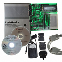
Manufacturer Part Number
M68EVB908GB60E
Description
BOARD EVAL FOR MC9S08GB60
Manufacturer
Freescale Semiconductor
Type
MCUr
Datasheet
1.M68EVB908GB60E.pdf
(290 pages)
Specifications of M68EVB908GB60E
Contents
Module and Misc Hardware
Processor To Be Evaluated
MC9S08GB
Data Bus Width
8 bit
Interface Type
RS-232
Silicon Manufacturer
Freescale
Core Architecture
HCS08
Core Sub-architecture
HCS08
Silicon Core Number
MC9S08
Silicon Family Name
S08GB
Kit Contents
GB60 Evaluation Kit
Rohs Compliant
Yes
For Use With/related Products
MC9S08GB60
Lead Free Status / RoHS Status
Lead free / RoHS Compliant


BIDIROE — Bidirectional Mode Output Enable
SPISWAI — SPI Stop in Wait Mode
SPC0 — SPI Pin Control 0
12.4.3
This register is used to set the prescaler and bit rate divisor for an SPI master. This register may be read or
written at any time.
SPPR2:SPPR1:SPPR0 — SPI Baud Rate Prescale Divisor
Freescale Semiconductor
When bidirectional mode is enabled by SPI pin control 0 (SPC0) = 1, BIDIROE determines whether
the SPI data output driver is enabled to the single bidirectional SPI I/O pin. Depending on whether the
SPI is configured as a master or a slave, it uses either the MOSI1 (MOMI) or MISO1 (SISO) pin,
respectively, as the single SPI data I/O pin. When SPC0 = 0, BIDIROE has no meaning or effect.
The SPC0 bit chooses single-wire bidirectional mode. If MSTR = 0 (slave mode), the SPI uses the
MISO1 (SISO) pin for bidirectional SPI data transfers. If MSTR = 1 (master mode), the SPI uses the
MOSI1 (MOMI) pin for bidirectional SPI data transfers. When SPC0 = 1, BIDIROE is used to enable
or disable the output driver for the single bidirectional SPI I/O pin.
This 3-bit field selects one of eight divisors for the SPI baud rate prescaler as shown in
input to this prescaler is the bus rate clock (BUSCLK). The output of this prescaler drives the input of
the SPI baud rate divider (see
1 = SPI I/O pin enabled as an output.
0 = Output driver disabled so SPI data I/O pin acts as an input.
1 = SPI clocks stop when the MCU enters wait mode.
0 = SPI clocks continue to operate in wait mode.
1 = SPI configured for single-wire bidirectional operation.
0 = SPI uses separate pins for data input and data output.
SPI Baud Rate Register (SPI1BR)
Reset:
Read:
Write:
Figure 12-9. SPI Baud Rate Register (SPI1BR)
Bit 7
0
0
Figure
MC9S08GB/GT Data Sheet, Rev. 2.3
= Unimplemented or Reserved
SPPR2
6
0
12-4).
SPPR1
5
0
SPPR0
4
0
3
0
0
SPR2
2
0
SPI Registers and Control Bits
SPR1
1
0
Table
SPR0
Bit 0
0
12-2. The
199
Related parts for M68EVB908GB60E
Image
Part Number
Description
Manufacturer
Datasheet
Request
R

Part Number:
Description:
Manufacturer:
Freescale Semiconductor, Inc
Datasheet:
Part Number:
Description:
Manufacturer:
Freescale Semiconductor, Inc
Datasheet:
Part Number:
Description:
Manufacturer:
Freescale Semiconductor, Inc
Datasheet:
Part Number:
Description:
Manufacturer:
Freescale Semiconductor, Inc
Datasheet:
Part Number:
Description:
Manufacturer:
Freescale Semiconductor, Inc
Datasheet:
Part Number:
Description:
Manufacturer:
Freescale Semiconductor, Inc
Datasheet:
Part Number:
Description:
Manufacturer:
Freescale Semiconductor, Inc
Datasheet:
Part Number:
Description:
Manufacturer:
Freescale Semiconductor, Inc
Datasheet:
Part Number:
Description:
Manufacturer:
Freescale Semiconductor, Inc
Datasheet:
Part Number:
Description:
Manufacturer:
Freescale Semiconductor, Inc
Datasheet:
Part Number:
Description:
Manufacturer:
Freescale Semiconductor, Inc
Datasheet:
Part Number:
Description:
Manufacturer:
Freescale Semiconductor, Inc
Datasheet:
Part Number:
Description:
Manufacturer:
Freescale Semiconductor, Inc
Datasheet:
Part Number:
Description:
Manufacturer:
Freescale Semiconductor, Inc
Datasheet:
Part Number:
Description:
Manufacturer:
Freescale Semiconductor, Inc
Datasheet: