M30879FLGP#U3 Renesas Electronics America, M30879FLGP#U3 Datasheet - Page 110
M30879FLGP#U3
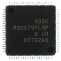
Manufacturer Part Number
M30879FLGP#U3
Description
IC M32C/87 MCU FLASH 100LQFP
Manufacturer
Renesas Electronics America
Series
M16C™ M32C/80r
Specifications of M30879FLGP#U3
Core Size
16/32-Bit
Program Memory Size
1MB (1M x 8)
Core Processor
M32C/80
Speed
32MHz
Connectivity
CAN, EBI/EMI, I²C, IEBus, IrDA, SIO, UART/USART
Peripherals
DMA, POR, PWM, WDT
Number Of I /o
85
Program Memory Type
FLASH
Ram Size
48K x 8
Voltage - Supply (vcc/vdd)
3 V ~ 5.5 V
Data Converters
A/D 26x10b; D/A 2x8b
Oscillator Type
Internal
Operating Temperature
-40°C ~ 85°C
Package / Case
100-LQFP
Controller Family/series
M32C
No. Of I/o's
85
Ram Memory Size
48KB
Cpu Speed
32MHz
No. Of Timers
2
Digital Ic Case Style
LQFP
Embedded Interface Type
CAN, I2C, UART
Rohs Compliant
Yes
Lead Free Status / RoHS Status
Lead free / RoHS Compliant
For Use With
R0K330879S001BE - KIT DEV RSK M32C/87R0K330879S000BE - KIT DEV RSK M32C/87
Eeprom Size
-
Lead Free Status / RoHS Status
Lead free / RoHS Compliant, Lead free / RoHS Compliant
Available stocks
Company
Part Number
Manufacturer
Quantity
Price

Part Number:
M30879FLGP#U3M30879FLGP#U5
Manufacturer:
Renesas Electronics America
Quantity:
10 000


M32C/87 Group (M32C/87, M32C/87A, M32C/87B)
REJ09B0180-0151 Rev.1.51 Jul 31, 2008
Page 86 of 587
Figure 9.6
PLL Control Register 0
PLL Control Register 1
b7 b6 b5 b4
b7
0 0 0
b6 b5 b4
NOTES:
1
NOTES:
1. Set the PLC1 register after the PRC0 bit in the PRCR register is set to 1 (write enable).
2. If the PM21 bit in the PM2 register is set to 1 (disables a clock change), a write to the the PLC1 register has no effect.
3. Set the PLC1 register while the PLC07 bit is 0 (PLL stopped).The PLC1 register can be written only once.
4. Set registers PLC0 and PLC1 simultaneously in 16-bit units.
0
1. Set the PLC0 register after the PRC0 bit in the PRCR register is set to 1 (write enable).
2. If the PM21 bit in the PM2 register is set to 1 (disables a clock change), a write to the PLC0 register has no effect.
3. Set bits PLC02 to PLC00 while the PLC07 bit is 0. Bits PLC02 to PLC00 can be written only once.
4. Enter wait mode or stop mode after the CM17 bit is set to 0 (main clock as CPU clock source) and then the PLC07 bit to 0.
5. Set registers PLC0 and PLC1 simultaneously in 16-bit units .
1
b3
b3
0
b2
b2
PLC0 Register, PLC1 Register
b1
b1
1 0
b0
b0
Bit Symbol
Bit Symbol
(b7-b5)
PLC00
PLC01
PLC02
PLC07
PLC12
Symbol
PLC0
(b3)
(b4)
(b5)
(b6)
(b0)
(b1)
(b3)
(b4)
Syambol
PLC1
−
−
−
−
−
−
−
−
−
(1, 2, 3, 4)
(1, 2, 5)
PLL clock division select bit
Reserved bit
Reserved bit
Reserved bit
Reserved bit
Reserved bits
Programmable counter
select bits
Reserved bit
Reserved bit
Reserved bit
Reserved bit
Operation enable bit
(3)
Bit Name
Bit Name
(4)
Address
0026h
Address
0027h
0: Divide-by-2
1: Divide-by-3
Set to 0
Set to 1
Set to 0
Read as undefined value
Set to 0
The VCO clock is the main clock multiplied by
the following variables.
b2 b1 b0
0 1 1: Multiply-by-6
1 0 0: Multiply-by-8
Do not set to values other than the above
Read as undefined value
Set to 1
Set to 0
Set to 1
0: PLL stops
1: PLL runs
Function
Function
9. Clock Generation Circuits
After Reset
0001 X010b
After Reset
000X 0000b
RW
RW
RW
RW
RW
RW
RW
RW
RW
RW
RW
RW
RW
RW
−
−
Related parts for M30879FLGP#U3
Image
Part Number
Description
Manufacturer
Datasheet
Request
R

Part Number:
Description:
KIT STARTER FOR M16C/29
Manufacturer:
Renesas Electronics America
Datasheet:

Part Number:
Description:
KIT STARTER FOR R8C/2D
Manufacturer:
Renesas Electronics America
Datasheet:

Part Number:
Description:
R0K33062P STARTER KIT
Manufacturer:
Renesas Electronics America
Datasheet:

Part Number:
Description:
KIT STARTER FOR R8C/23 E8A
Manufacturer:
Renesas Electronics America
Datasheet:

Part Number:
Description:
KIT STARTER FOR R8C/25
Manufacturer:
Renesas Electronics America
Datasheet:

Part Number:
Description:
KIT STARTER H8S2456 SHARPE DSPLY
Manufacturer:
Renesas Electronics America
Datasheet:

Part Number:
Description:
KIT STARTER FOR R8C38C
Manufacturer:
Renesas Electronics America
Datasheet:

Part Number:
Description:
KIT STARTER FOR R8C35C
Manufacturer:
Renesas Electronics America
Datasheet:

Part Number:
Description:
KIT STARTER FOR R8CL3AC+LCD APPS
Manufacturer:
Renesas Electronics America
Datasheet:
Part Number:
Description:
KIT STARTER FOR RX610
Manufacturer:
Renesas Electronics America
Datasheet:

Part Number:
Description:
KIT STARTER FOR R32C/118
Manufacturer:
Renesas Electronics America
Datasheet:

Part Number:
Description:
KIT DEV RSK-R8C/26-29
Manufacturer:
Renesas Electronics America
Datasheet:

Part Number:
Description:
KIT STARTER FOR SH7124
Manufacturer:
Renesas Electronics America
Datasheet:

Part Number:
Description:
KIT STARTER FOR H8SX/1622
Manufacturer:
Renesas Electronics America
Datasheet:

Part Number:
Description:
KIT DEV FOR SH7203
Manufacturer:
Renesas Electronics America
Datasheet: