M30879FLGP#U3 Renesas Electronics America, M30879FLGP#U3 Datasheet - Page 587
M30879FLGP#U3
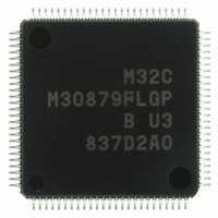
Manufacturer Part Number
M30879FLGP#U3
Description
IC M32C/87 MCU FLASH 100LQFP
Manufacturer
Renesas Electronics America
Series
M16C™ M32C/80r
Specifications of M30879FLGP#U3
Core Size
16/32-Bit
Program Memory Size
1MB (1M x 8)
Core Processor
M32C/80
Speed
32MHz
Connectivity
CAN, EBI/EMI, I²C, IEBus, IrDA, SIO, UART/USART
Peripherals
DMA, POR, PWM, WDT
Number Of I /o
85
Program Memory Type
FLASH
Ram Size
48K x 8
Voltage - Supply (vcc/vdd)
3 V ~ 5.5 V
Data Converters
A/D 26x10b; D/A 2x8b
Oscillator Type
Internal
Operating Temperature
-40°C ~ 85°C
Package / Case
100-LQFP
Controller Family/series
M32C
No. Of I/o's
85
Ram Memory Size
48KB
Cpu Speed
32MHz
No. Of Timers
2
Digital Ic Case Style
LQFP
Embedded Interface Type
CAN, I2C, UART
Rohs Compliant
Yes
Lead Free Status / RoHS Status
Lead free / RoHS Compliant
For Use With
R0K330879S001BE - KIT DEV RSK M32C/87R0K330879S000BE - KIT DEV RSK M32C/87
Eeprom Size
-
Lead Free Status / RoHS Status
Lead free / RoHS Compliant, Lead free / RoHS Compliant
Available stocks
Company
Part Number
Manufacturer
Quantity
Price

Part Number:
M30879FLGP#U3M30879FLGP#U5
Manufacturer:
Renesas Electronics America
Quantity:
10 000


M32C/87 Group (M32C/87, M32C/87A, M32C/87B)
REJ09B0180-0151 Rev.1.51 Jul 31, 2008
Page 563 of 587
28.5.4.3
The followings are suggestions to reduce power consumption when programming or designing systems.
Ports:
A/D converter:
D/A converter:
Peripheral function clock stop:
•
•
•
•
•
Through current may flow into floating input pins. Set unassigned pins to input mode and connect them to
VSS via a resistor (pull down), or set unassigned pins to output mode and leave them open.
When the A/D conversion is not performed, set the VCUT bit in the AD0CON1 register to 0 (VREF not
connected). When the A/D conversion is performed, set the VCUT bit to 1 (VREF connection) and wait
1 μs or more to start the A/D conversion.
When the D/A conversion is not performed, set the DAiE bit (i = 0, 1) in the DACON register to 0 (output
disabled) and registers DACON1 and DAi to 00h.
When entering wait mode from main clock mode, on-chip oscillator mode, or on-chip oscillator low-power
consumption mode, power consumption can be reduced by setting the CM02 bit in the CM0 register to 1 to
stop peripheral function clock source (fPFC). However, fC32 does not stop by setting the CM02 bit to 1.
In low-speed mode, do not set the CM02 bit to 1 (peripheral clock stops in wait mode) when entering wait
mode.
(Technical update: TN-M16C-69-0104)
Suggestions to Reduce Power Consumption
28. Usage Notes
Related parts for M30879FLGP#U3
Image
Part Number
Description
Manufacturer
Datasheet
Request
R

Part Number:
Description:
KIT STARTER FOR M16C/29
Manufacturer:
Renesas Electronics America
Datasheet:

Part Number:
Description:
KIT STARTER FOR R8C/2D
Manufacturer:
Renesas Electronics America
Datasheet:

Part Number:
Description:
R0K33062P STARTER KIT
Manufacturer:
Renesas Electronics America
Datasheet:

Part Number:
Description:
KIT STARTER FOR R8C/23 E8A
Manufacturer:
Renesas Electronics America
Datasheet:

Part Number:
Description:
KIT STARTER FOR R8C/25
Manufacturer:
Renesas Electronics America
Datasheet:

Part Number:
Description:
KIT STARTER H8S2456 SHARPE DSPLY
Manufacturer:
Renesas Electronics America
Datasheet:

Part Number:
Description:
KIT STARTER FOR R8C38C
Manufacturer:
Renesas Electronics America
Datasheet:

Part Number:
Description:
KIT STARTER FOR R8C35C
Manufacturer:
Renesas Electronics America
Datasheet:

Part Number:
Description:
KIT STARTER FOR R8CL3AC+LCD APPS
Manufacturer:
Renesas Electronics America
Datasheet:
Part Number:
Description:
KIT STARTER FOR RX610
Manufacturer:
Renesas Electronics America
Datasheet:

Part Number:
Description:
KIT STARTER FOR R32C/118
Manufacturer:
Renesas Electronics America
Datasheet:

Part Number:
Description:
KIT DEV RSK-R8C/26-29
Manufacturer:
Renesas Electronics America
Datasheet:

Part Number:
Description:
KIT STARTER FOR SH7124
Manufacturer:
Renesas Electronics America
Datasheet:

Part Number:
Description:
KIT STARTER FOR H8SX/1622
Manufacturer:
Renesas Electronics America
Datasheet:

Part Number:
Description:
KIT DEV FOR SH7203
Manufacturer:
Renesas Electronics America
Datasheet: