M30879FLGP#U3 Renesas Electronics America, M30879FLGP#U3 Datasheet - Page 172
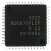
M30879FLGP#U3
Manufacturer Part Number
M30879FLGP#U3
Description
IC M32C/87 MCU FLASH 100LQFP
Manufacturer
Renesas Electronics America
Series
M16C™ M32C/80r
Specifications of M30879FLGP#U3
Core Size
16/32-Bit
Program Memory Size
1MB (1M x 8)
Core Processor
M32C/80
Speed
32MHz
Connectivity
CAN, EBI/EMI, I²C, IEBus, IrDA, SIO, UART/USART
Peripherals
DMA, POR, PWM, WDT
Number Of I /o
85
Program Memory Type
FLASH
Ram Size
48K x 8
Voltage - Supply (vcc/vdd)
3 V ~ 5.5 V
Data Converters
A/D 26x10b; D/A 2x8b
Oscillator Type
Internal
Operating Temperature
-40°C ~ 85°C
Package / Case
100-LQFP
Controller Family/series
M32C
No. Of I/o's
85
Ram Memory Size
48KB
Cpu Speed
32MHz
No. Of Timers
2
Digital Ic Case Style
LQFP
Embedded Interface Type
CAN, I2C, UART
Rohs Compliant
Yes
Lead Free Status / RoHS Status
Lead free / RoHS Compliant
For Use With
R0K330879S001BE - KIT DEV RSK M32C/87R0K330879S000BE - KIT DEV RSK M32C/87
Eeprom Size
-
Lead Free Status / RoHS Status
Lead free / RoHS Compliant, Lead free / RoHS Compliant
Available stocks
Company
Part Number
Manufacturer
Quantity
Price

Part Number:
M30879FLGP#U3M30879FLGP#U5
Manufacturer:
Renesas Electronics America
Quantity:
10 000


M32C/87 Group (M32C/87, M32C/87A, M32C/87B)
REJ09B0180-0151 Rev.1.51 Jul 31, 2008
Page 148 of 587
13.1
13.1.1
13.1.2
13.1.3
13.1.4
The transfer cycle is composed of bus cycles to read data from source address (source read) and bus cycles to write
data to destination address (destination write). The number of read and write bus cycles depends on the locations of
source and destination addresses. In memory expansion mode and microprocessor mode, the number of read and
write bus cycles also depends on DS register setting. Software wait state insertion and the RDY signal can extend
the number of the bus cycles.
When a 16-bit data is transferred with a 16-bit data bus and a source address starts with an odd address, the
source-read cycle is added by one bus cycle, compared to a source address starting with an even address.
When a 16-bit data is transferred with a 16-bit data bus and a destination address starts with an odd address, the
destination-write cycle is added by one bus cycle, compared to a destination address starting with an even
address.
In an external space in memory expansion mode and microprocessor mode, the transfer cycle varies depending
on the data bus width of the source and destination addresses. See Figure 8.1 for details about the DS register.
When accessing the SFR area or memory space that requires wait states, the number of bus clocks (BCLK) is
increased by software wait states.
In memory expansion mode and microprocessor mode, the RDY signal affects the number of the bus cycles if a
source address or destination address is in an external space. Refer to 8.2.6 RDY Signal for details.
Transfer Cycles
•
•
•
When a 16-bit data is transferred accessing both source address and destination address with an 8-bit data
bus (the DSi bit in the DS register is set to 0 (i = 0 to 3)), an 8-bit data will be transferred twice. Therefore,
two bus cycles are required for reading and another two bus cycles for writing.
When a 16-bit data is transferred accessing a source address with an 8-bit data bus (the DSi bit is set to 0)
and a destination address with a 16-bit data bus, an 8-bit data will be read twice but be written once as 16-
bit data. Therefore, two bus cycles are required for reading and one bus cycle for writing.
When a 16-bit data is transferred accessing a source address with a 16-bit data bus (the DSi bit is set to 1)
and a destination address with an 8-bit data bus, a 16-bit data will be read once and an 8-bit data will be
written twice. Therefore, one bus cycle is required for reading and two bus cycles for writing.
Effect of Source and Destination Addresses
Effect of the DS Register
Effect of Software Wait State
Effect of the RDY Signal
13. DMAC
Related parts for M30879FLGP#U3
Image
Part Number
Description
Manufacturer
Datasheet
Request
R

Part Number:
Description:
KIT STARTER FOR M16C/29
Manufacturer:
Renesas Electronics America
Datasheet:

Part Number:
Description:
KIT STARTER FOR R8C/2D
Manufacturer:
Renesas Electronics America
Datasheet:

Part Number:
Description:
R0K33062P STARTER KIT
Manufacturer:
Renesas Electronics America
Datasheet:

Part Number:
Description:
KIT STARTER FOR R8C/23 E8A
Manufacturer:
Renesas Electronics America
Datasheet:

Part Number:
Description:
KIT STARTER FOR R8C/25
Manufacturer:
Renesas Electronics America
Datasheet:

Part Number:
Description:
KIT STARTER H8S2456 SHARPE DSPLY
Manufacturer:
Renesas Electronics America
Datasheet:

Part Number:
Description:
KIT STARTER FOR R8C38C
Manufacturer:
Renesas Electronics America
Datasheet:

Part Number:
Description:
KIT STARTER FOR R8C35C
Manufacturer:
Renesas Electronics America
Datasheet:

Part Number:
Description:
KIT STARTER FOR R8CL3AC+LCD APPS
Manufacturer:
Renesas Electronics America
Datasheet:
Part Number:
Description:
KIT STARTER FOR RX610
Manufacturer:
Renesas Electronics America
Datasheet:

Part Number:
Description:
KIT STARTER FOR R32C/118
Manufacturer:
Renesas Electronics America
Datasheet:

Part Number:
Description:
KIT DEV RSK-R8C/26-29
Manufacturer:
Renesas Electronics America
Datasheet:

Part Number:
Description:
KIT STARTER FOR SH7124
Manufacturer:
Renesas Electronics America
Datasheet:

Part Number:
Description:
KIT STARTER FOR H8SX/1622
Manufacturer:
Renesas Electronics America
Datasheet:

Part Number:
Description:
KIT DEV FOR SH7203
Manufacturer:
Renesas Electronics America
Datasheet: