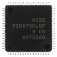
M30879FLGP#U3 Renesas Electronics America, M30879FLGP#U3 Datasheet - Page 281

M30879FLGP#U3
Manufacturer Part Number
M30879FLGP#U3
Description
IC M32C/87 MCU FLASH 100LQFP
Manufacturer
Renesas Electronics America
Series
M16C™ M32C/80r
Specifications of M30879FLGP#U3
Core Size
16/32-Bit
Program Memory Size
1MB (1M x 8)
Core Processor
M32C/80
Speed
32MHz
Connectivity
CAN, EBI/EMI, I²C, IEBus, IrDA, SIO, UART/USART
Peripherals
DMA, POR, PWM, WDT
Number Of I /o
85
Program Memory Type
FLASH
Ram Size
48K x 8
Voltage - Supply (vcc/vdd)
3 V ~ 5.5 V
Data Converters
A/D 26x10b; D/A 2x8b
Oscillator Type
Internal
Operating Temperature
-40°C ~ 85°C
Package / Case
100-LQFP
Controller Family/series
M32C
No. Of I/o's
85
Ram Memory Size
48KB
Cpu Speed
32MHz
No. Of Timers
2
Digital Ic Case Style
LQFP
Embedded Interface Type
CAN, I2C, UART
Rohs Compliant
Yes
Lead Free Status / RoHS Status
Lead free / RoHS Compliant
For Use With
R0K330879S001BE - KIT DEV RSK M32C/87R0K330879S000BE - KIT DEV RSK M32C/87
Eeprom Size
-
Lead Free Status / RoHS Status
Lead free / RoHS Compliant, Lead free / RoHS Compliant
Available stocks
Company
Part Number
Manufacturer
Quantity
Price
Part Number:
M30879FLGP#U3M30879FLGP#U5
Manufacturer:
Renesas Electronics America
Quantity:
10 000
- Current page: 281 of 629
- Download datasheet (16Mb)
M32C/87 Group (M32C/87, M32C/87A, M32C/87B)
REJ09B0180-0151 Rev.1.51 Jul 31, 2008
Page 257 of 587
Figure 17.28
17.1.4.1 Master Mode
17.1.4.2 Slave Mode
Master mode is entered when the DINC bit in the UiSMR3 register (i = 0 to 4) is set to 1. The following pins are
used in master mode.
To use the SS function, set the SSE bit in the UiSMR3 register to 1. A transmit and receive operation is
performed while an “H” is applied to the SSi pin. If an “L” is applied to the SSi pin, the ERR bit in the UiSMR3
register becomes 1 (mode error occurred) and pins CLKi and TXDi are placed in high-impedance states. Set the
UiIRS bit in the UiC1 register to 1 (Transmit completion as interrupt source) to verify whether a mode error has
occurred or not by checking the EER bit in the transmission complete interrupt routine. To resume serial
communication after a mode error occurs, set the ERR bit to 0 (no mode error) while an “H” signal is applied to
the SSi pin. Pins TXDi and CLKi become in output mode.
Slave mode is entered when the DINC bit in the UiSMR3 register is set to 0. The following pins are used in
slave mode.
To use the SS function, set the SSE bit in the UiSMR3 register to 1. When an “L” signal is applied to the SSi
input pin, the serial clock input is enabled, and a transmit and receive operation becomes available. When an
“H” signal is applied to the SSi pin, the serial clock input to the CLKi pin is ignored and the STXDi pin is
placed in a high-impedance state.
•
•
•
•
•
•
TXDi: transmit data output
RXDi: receive data input
CLKi: serial clock output
STXDi: transmit data output
SRXDi: receive data input
CLKi: serial clock input
Serial Bus Communication Control with SSi Pin
(Master)
MCU
P9_1(RXD3)
P9_2(TXD3)
P9_0(CLK3)
P9_3(SS3)
P1_3
P1_2
P9_3(SS3)
P9_0(CLK3)
P9_1(STXD3)
P9_2(SRXD3)
P9_3(SS3)
P9_0(CLK3)
P9_1(STXD3)
P9_2(SRXD3)
17. Serial Interfaces (UART0 to UART4)
(Slave)
(Slave)
MCU
MCU
Related parts for M30879FLGP#U3
Image
Part Number
Description
Manufacturer
Datasheet
Request
R

Part Number:
Description:
KIT STARTER FOR M16C/29
Manufacturer:
Renesas Electronics America
Datasheet:

Part Number:
Description:
KIT STARTER FOR R8C/2D
Manufacturer:
Renesas Electronics America
Datasheet:

Part Number:
Description:
R0K33062P STARTER KIT
Manufacturer:
Renesas Electronics America
Datasheet:

Part Number:
Description:
KIT STARTER FOR R8C/23 E8A
Manufacturer:
Renesas Electronics America
Datasheet:

Part Number:
Description:
KIT STARTER FOR R8C/25
Manufacturer:
Renesas Electronics America
Datasheet:

Part Number:
Description:
KIT STARTER H8S2456 SHARPE DSPLY
Manufacturer:
Renesas Electronics America
Datasheet:

Part Number:
Description:
KIT STARTER FOR R8C38C
Manufacturer:
Renesas Electronics America
Datasheet:

Part Number:
Description:
KIT STARTER FOR R8C35C
Manufacturer:
Renesas Electronics America
Datasheet:

Part Number:
Description:
KIT STARTER FOR R8CL3AC+LCD APPS
Manufacturer:
Renesas Electronics America
Datasheet:

Part Number:
Description:
KIT STARTER FOR RX610
Manufacturer:
Renesas Electronics America
Datasheet:

Part Number:
Description:
KIT STARTER FOR R32C/118
Manufacturer:
Renesas Electronics America
Datasheet:

Part Number:
Description:
KIT DEV RSK-R8C/26-29
Manufacturer:
Renesas Electronics America
Datasheet:

Part Number:
Description:
KIT STARTER FOR SH7124
Manufacturer:
Renesas Electronics America
Datasheet:

Part Number:
Description:
KIT STARTER FOR H8SX/1622
Manufacturer:
Renesas Electronics America
Datasheet:

Part Number:
Description:
KIT DEV FOR SH7203
Manufacturer:
Renesas Electronics America
Datasheet:


