Z8F2480AN020SG Zilog, Z8F2480AN020SG Datasheet - Page 78
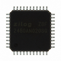
Z8F2480AN020SG
Manufacturer Part Number
Z8F2480AN020SG
Description
MCU 8BIT 24KB FLASH 44LQFP
Manufacturer
Zilog
Series
Encore!® XP®r
Specifications of Z8F2480AN020SG
Core Processor
Z8
Core Size
8-Bit
Speed
20MHz
Connectivity
I²C, IrDA, LIN, SPI, UART/USART
Peripherals
Brown-out Detect/Reset, LED, LVD, POR, PWM, Temp Sensor, WDT
Number Of I /o
37
Program Memory Size
24KB (24K x 8)
Program Memory Type
FLASH
Ram Size
3K x 8
Voltage - Supply (vcc/vdd)
1.8 V ~ 3.6 V
Data Converters
A/D 8x10b
Oscillator Type
Internal
Operating Temperature
0°C ~ 70°C
Package / Case
44-LQFP
Processor Series
Z8F248x
Core
eZ8
Data Bus Width
8 bit
Data Ram Size
2 KB
Interface Type
I2C, SPI, UART
Maximum Clock Frequency
20 MHz
Number Of Programmable I/os
37
Number Of Timers
3
Maximum Operating Temperature
+ 70 C
Mounting Style
SMD/SMT
Minimum Operating Temperature
0 C
On-chip Adc
10 bit, 8 Channel
For Use With
770-1002 - ISP 4PORT ZILOG Z8 ENCORE! MCU269-4643 - KIT DEV Z8 ENCORE XP 28-PIN269-4630 - DEV KIT FOR Z8 ENCORE 8K/4K269-4629 - KIT DEV Z8 ENCORE XP 28-PIN269-4628 - KIT DEV Z8 ENCORE XP 8-PIN
Lead Free Status / RoHS Status
Lead free / RoHS Compliant
Eeprom Size
-
Lead Free Status / Rohs Status
Details
Other names
269-4676
Available stocks
Company
Part Number
Manufacturer
Quantity
Price
Company:

Part Number:
Z8F2480AN020SG
Manufacturer:
Zilog
Quantity:
85


Table 21. Port A–E Data Direction Subregisters (PxDD)
Table 22. Port A–E Alternate Function Subregisters (PxAF)
BITS
FIELD
RESET
R/W
ADDR
BITS
FIELD
RESET
R/W
ADDR
PS025011-1010
Caution:
Port A
DD7
R/W
AF7
If 01H in Port A–E Address Register, accessible through the Port A–E Control Register
If 02H in Port A–D Address Register, accessible through the Port A–E Control Register
7
1
7
DD[7:0]—Data Direction
These bits control the direction of the associated port pin. Port Alternate Function
operation overrides the Data Direction register setting.
0 = Output. Data in the Port A–E Output Data register is driven onto the port pin.
1 = Input. The port pin is sampled and the value written into the Port A–E Input Data
The Port A–E Alternate Function subregister (see
Port A–E Control register by writing
Alternate Function subregisters enable the alternate function selection on pins. If disabled,
pins functions as GPIO. If enabled, select one of the four alternate functions using
Alternate Function set subregisters 1 and 2 as described in
Set 1 Subregisters
67
Functions
AF[7:0]—Port Alternate Function enabled
0 = The port pin is in NORMAL mode and the DDx bit in the Port A–E Data Direction
–
E Alternate Function Subregisters
.
Do not enable alternate functions for GPIO port pins for which there is no associated
alternate function. Failure to follow this guideline results in unpredictable operation.
To determine the alternate function associated with each port pin, see
Register. The output driver is tristated.
subregister determines the direction of the pin.
DD6
R/W
AF6
on page 50.
6
1
6
on page 67 and
00H (Ports A–C); 01H (Port D); 00H (Port E);
DD5
R/W
AF5
5
1
5
P R E L I M I N A R Y
DD4
R/W
Port A–E Alternate Function Set 2 Subregisters
AF4
4
1
4
02H
R/W
to the Port A–E Address register. The Port A–E
DD3
R/W
AF3
3
1
3
Table
Z8 Encore! XP
22) is accessed through the
DD2
R/W
AF2
Port A–E Alternate Function
2
1
2
General-Purpose Input/Output
Product Specification
DD1
R/W
AF1
1
1
1
®
GPIO Alternate
F1680 Series
on page
DD0
R/W
AF0
0
1
0
64
Related parts for Z8F2480AN020SG
Image
Part Number
Description
Manufacturer
Datasheet
Request
R

Part Number:
Description:
Communication Controllers, ZILOG INTELLIGENT PERIPHERAL CONTROLLER (ZIP)
Manufacturer:
Zilog, Inc.
Datasheet:

Part Number:
Description:
KIT DEV FOR Z8 ENCORE 16K TO 64K
Manufacturer:
Zilog
Datasheet:

Part Number:
Description:
KIT DEV Z8 ENCORE XP 28-PIN
Manufacturer:
Zilog
Datasheet:

Part Number:
Description:
DEV KIT FOR Z8 ENCORE 8K/4K
Manufacturer:
Zilog
Datasheet:

Part Number:
Description:
KIT DEV Z8 ENCORE XP 28-PIN
Manufacturer:
Zilog
Datasheet:

Part Number:
Description:
DEV KIT FOR Z8 ENCORE 4K TO 8K
Manufacturer:
Zilog
Datasheet:
Part Number:
Description:
CMOS Z8 microcontroller. ROM 16 Kbytes, RAM 256 bytes, speed 16 MHz, 32 lines I/O, 3.0V to 5.5V
Manufacturer:
Zilog, Inc.
Datasheet:
Part Number:
Description:
Low-cost microcontroller. 512 bytes ROM, 61 bytes RAM, 8 MHz
Manufacturer:
Zilog, Inc.
Datasheet:
Part Number:
Description:
Z8 4K OTP Microcontroller
Manufacturer:
Zilog, Inc.
Datasheet:
Part Number:
Description:
CMOS SUPER8 ROMLESS MCU
Manufacturer:
Zilog, Inc.
Datasheet:
Part Number:
Description:
SL1866 CMOSZ8 OTP Microcontroller
Manufacturer:
Zilog, Inc.
Datasheet:
Part Number:
Description:
SL1866 CMOSZ8 OTP Microcontroller
Manufacturer:
Zilog, Inc.
Datasheet:
Part Number:
Description:
OTP (KB) = 1, RAM = 125, Speed = 12, I/O = 14, 8-bit Timers = 2, Comm Interfaces Other Features = Por, LV Protect, Voltage = 4.5-5.5V
Manufacturer:
Zilog, Inc.
Datasheet:
Part Number:
Description:
Manufacturer:
Zilog, Inc.
Datasheet: