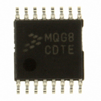
MC9S08QG8CDTE Freescale Semiconductor, MC9S08QG8CDTE Datasheet - Page 255

MC9S08QG8CDTE
Manufacturer Part Number
MC9S08QG8CDTE
Description
IC MCU 8K FLASH 10MHZ 16-TSSOP
Manufacturer
Freescale Semiconductor
Series
HCS08r
Datasheet
1.MC9S08QG8CDTER.pdf
(314 pages)
Specifications of MC9S08QG8CDTE
Core Processor
HCS08
Core Size
8-Bit
Speed
20MHz
Connectivity
I²C, SCI, SPI
Peripherals
LVD, POR, PWM, WDT
Number Of I /o
12
Program Memory Size
8KB (8K x 8)
Program Memory Type
FLASH
Ram Size
512 x 8
Voltage - Supply (vcc/vdd)
1.8 V ~ 3.6 V
Data Converters
A/D 8x10b
Oscillator Type
Internal
Operating Temperature
-40°C ~ 85°C
Package / Case
16-TSSOP
Cpu Family
HCS08
Device Core Size
8b
Frequency (max)
20MHz
Interface Type
I2C/SCI/SPI
Total Internal Ram Size
512Byte
# I/os (max)
12
Number Of Timers - General Purpose
1
Operating Supply Voltage (typ)
2.5/3.3V
Operating Supply Voltage (max)
3.6V
Operating Supply Voltage (min)
1.8V
On-chip Adc
8-chx10-bit
Instruction Set Architecture
CISC
Operating Temp Range
-40C to 85C
Operating Temperature Classification
Industrial
Mounting
Surface Mount
Pin Count
16
Package Type
TSSOP
Processor Series
S08QG
Core
HCS08
Data Bus Width
8 bit
Data Ram Size
512 B
Maximum Clock Frequency
20 MHz
Number Of Programmable I/os
12
Number Of Timers
1
Operating Supply Voltage
1.8 V to 3.6 V
Maximum Operating Temperature
+ 85 C
Mounting Style
SMD/SMT
3rd Party Development Tools
EWS08
Development Tools By Supplier
DEMO9S08QG8E
Minimum Operating Temperature
- 40 C
Package
16TSSOP
Family Name
HCS08
Maximum Speed
20 MHz
For Use With
DEMO9S08QG8E - BOARD DEMO FOR MC9S08QG8
Lead Free Status / RoHS Status
Lead free / RoHS Compliant
Eeprom Size
-
Lead Free Status / Rohs Status
Compliant
Available stocks
Company
Part Number
Manufacturer
Quantity
Price
Company:
Part Number:
MC9S08QG8CDTE
Manufacturer:
ABB
Quantity:
101
Company:
Part Number:
MC9S08QG8CDTE
Manufacturer:
Freescale Semiconductor
Quantity:
41 991
Part Number:
MC9S08QG8CDTE
Manufacturer:
FREESCALE
Quantity:
20 000
the host must perform ((8 – CNT) – 1) dummy reads of the FIFO to advance it to the first significant entry
in the FIFO.
In most trigger modes, the information stored in the FIFO consists of 16-bit change-of-flow addresses. In
these cases, read DBGFH then DBGFL to get one coherent word of information out of the FIFO. Reading
DBGFL (the low-order byte of the FIFO data port) causes the FIFO to shift so the next word of information
is available at the FIFO data port. In the event-only trigger modes (see
8-bit data information is stored into the FIFO. In these cases, the high-order half of the FIFO (DBGFH) is
not used and data is read out of the FIFO by simply reading DBGFL. Each time DBGFL is read, the FIFO
is shifted so the next data value is available through the FIFO data port at DBGFL.
In trigger modes where the FIFO is storing change-of-flow addresses, there is a delay between CPU
addresses and the input side of the FIFO. Because of this delay, if the trigger event itself is a
change-of-flow address or a change-of-flow address appears during the next two bus cycles after a trigger
event starts the FIFO, it will not be saved into the FIFO. In the case of an end-trace, if the trigger event is
a change-of-flow, it will be saved as the last change-of-flow entry for that debug run.
The FIFO can also be used to generate a profile of executed instruction addresses when the debugger is
not armed. When ARM = 0, reading DBGFL causes the address of the most-recently fetched opcode to be
saved in the FIFO. To use the profiling feature, a host debugger would read addresses out of the FIFO by
reading DBGFH then DBGFL at regular periodic intervals. The first eight values would be discarded
because they correspond to the eight DBGFL reads needed to initially fill the FIFO. Additional periodic
reads of DBGFH and DBGFL return delayed information about executed instructions so the host debugger
can develop a profile of executed instruction addresses.
17.3.3
To minimize the amount of information stored in the FIFO, only information related to instructions that
cause a change to the normal sequential execution of instructions is stored. With knowledge of the source
and object code program stored in the target system, an external debugger system can reconstruct the path
of execution through many instructions from the change-of-flow information stored in the FIFO.
For conditional branch instructions where the branch is taken (branch condition was true), the source
address is stored (the address of the conditional branch opcode). Because BRA and BRN instructions are
not conditional, these events do not cause change-of-flow information to be stored in the FIFO.
Indirect JMP and JSR instructions use the current contents of the H:X index register pair to determine the
destination address, so the debug system stores the run-time destination address for any indirect JMP or
JSR. For interrupts, RTI, or RTS, the destination address is stored in the FIFO as change-of-flow
information.
17.3.4
Tagging is a term that refers to identifying an instruction opcode as it is fetched into the instruction queue,
but not taking any other action until and unless that instruction is actually executed by the CPU. This
distinction is important because any change-of-flow from a jump, branch, subroutine call, or interrupt
causes some instructions that have been fetched into the instruction queue to be thrown away without being
executed.
Freescale Semiconductor
Change-of-Flow Information
Tag vs. Force Breakpoints and Triggers
MC9S08QG8 and MC9S08QG4 Data Sheet, Rev. 5
Section 17.3.5, “Trigger
Development Support
Modes”),
253


