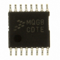
MC9S08QG8CDTE Freescale Semiconductor, MC9S08QG8CDTE Datasheet - Page 54

MC9S08QG8CDTE
Manufacturer Part Number
MC9S08QG8CDTE
Description
IC MCU 8K FLASH 10MHZ 16-TSSOP
Manufacturer
Freescale Semiconductor
Series
HCS08r
Datasheet
1.MC9S08QG8CDTER.pdf
(314 pages)
Specifications of MC9S08QG8CDTE
Core Processor
HCS08
Core Size
8-Bit
Speed
20MHz
Connectivity
I²C, SCI, SPI
Peripherals
LVD, POR, PWM, WDT
Number Of I /o
12
Program Memory Size
8KB (8K x 8)
Program Memory Type
FLASH
Ram Size
512 x 8
Voltage - Supply (vcc/vdd)
1.8 V ~ 3.6 V
Data Converters
A/D 8x10b
Oscillator Type
Internal
Operating Temperature
-40°C ~ 85°C
Package / Case
16-TSSOP
Cpu Family
HCS08
Device Core Size
8b
Frequency (max)
20MHz
Interface Type
I2C/SCI/SPI
Total Internal Ram Size
512Byte
# I/os (max)
12
Number Of Timers - General Purpose
1
Operating Supply Voltage (typ)
2.5/3.3V
Operating Supply Voltage (max)
3.6V
Operating Supply Voltage (min)
1.8V
On-chip Adc
8-chx10-bit
Instruction Set Architecture
CISC
Operating Temp Range
-40C to 85C
Operating Temperature Classification
Industrial
Mounting
Surface Mount
Pin Count
16
Package Type
TSSOP
Processor Series
S08QG
Core
HCS08
Data Bus Width
8 bit
Data Ram Size
512 B
Maximum Clock Frequency
20 MHz
Number Of Programmable I/os
12
Number Of Timers
1
Operating Supply Voltage
1.8 V to 3.6 V
Maximum Operating Temperature
+ 85 C
Mounting Style
SMD/SMT
3rd Party Development Tools
EWS08
Development Tools By Supplier
DEMO9S08QG8E
Minimum Operating Temperature
- 40 C
Package
16TSSOP
Family Name
HCS08
Maximum Speed
20 MHz
For Use With
DEMO9S08QG8E - BOARD DEMO FOR MC9S08QG8
Lead Free Status / RoHS Status
Lead free / RoHS Compliant
Eeprom Size
-
Lead Free Status / Rohs Status
Compliant
Available stocks
Company
Part Number
Manufacturer
Quantity
Price
Company:
Part Number:
MC9S08QG8CDTE
Manufacturer:
ABB
Quantity:
101
Company:
Part Number:
MC9S08QG8CDTE
Manufacturer:
Freescale Semiconductor
Quantity:
41 991
Part Number:
MC9S08QG8CDTE
Manufacturer:
FREESCALE
Quantity:
20 000
Chapter 4 Memory Map and Register Definition
must be programmed to logic 0 to enable block protection. Therefore the value 0xF8 must be programmed
into NVPROT to protect addresses 0xFA00 through 0xFFFF.
One use for block protection is to block protect an area of FLASH memory for a bootloader program. This
bootloader program then can be used to erase the rest of the FLASH memory and reprogram it. Because
the bootloader is protected, it remains intact even if MCU power is lost in the middle of an erase and
reprogram operation.
4.5.7
Whenever any block protection is enabled, the reset and interrupt vectors will be protected. Vector
redirection allows users to modify interrupt vector information without unprotecting bootloader and reset
vector space. Vector redirection is enabled by programming the FNORED bit in the NVOPT register
located at address 0xFFBF to zero. For redirection to occur, at least some portion but not all of the FLASH
memory must be block protected by programming the NVPROT register located at address 0xFFBD. All
of the interrupt vectors (memory locations 0xFFC0–0xFFFD) are redirected, though the reset vector
(0xFFFE:FFFF) is not.
For example, if 512 bytes of FLASH are protected, the protected address region is from 0xFE00 through
0xFFFF. The interrupt vectors (0xFFC0–0xFFFD) are redirected to the locations 0xFDC0–0xFDFD. Now,
if an SPI interrupt is taken for instance, the values in the locations 0xFDE0:FDE1 are used for the vector
instead of the values in the locations 0xFFE0:FFE1. This allows the user to reprogram the unprotected
portion of the FLASH with new program code including new interrupt vector values while leaving the
protected area, which includes the default vector locations, unchanged.
4.6
The MC9S08QG8/4 includes circuitry to prevent unauthorized access to the contents of FLASH and RAM
memory. When security is engaged, FLASH and RAM are considered secure resources. Direct-page
registers, high-page registers, and the background debug controller are considered unsecured resources.
Programs executing within secure memory have normal access to any MCU memory locations and
resources. Attempts to access a secure memory location with a program executing from an unsecured
memory space or through the background debug interface are blocked (writes are ignored and reads return
all 0s).
Security is engaged or disengaged based on the state of two nonvolatile register bits (SEC01:SEC00) in
the FOPT register. During reset, the contents of the nonvolatile location NVOPT are copied from FLASH
into the working FOPT register in high-page register space. A user engages security by programming the
NVOPT location which can be done at the same time the FLASH memory is programmed. The 1:0 state
disengages security and the other three combinations engage security. Notice the erased state (1:1) makes
52
Security
Vector Redirection
FPS7 FPS6 FPS5 FPS4 FPS3 FPS2 FPS1
A15
A14
A13
MC9S08QG8 and MC9S08QG4 Data Sheet, Rev. 5
Figure 4-4. Block Protection Mechanism
A12
A11
A10
A9
A8
1
A7 A6 A5 A4 A3 A2 A1 A0
1
1
1
1
1
1
Freescale Semiconductor
1
1


