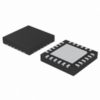
C8051F988-GM Silicon Laboratories Inc, C8051F988-GM Datasheet - Page 182

C8051F988-GM
Manufacturer Part Number
C8051F988-GM
Description
IC MCU 8BIT 4KB FLASH 24QFN
Manufacturer
Silicon Laboratories Inc
Series
C8051F9xxr
Specifications of C8051F988-GM
Program Memory Type
FLASH
Program Memory Size
4KB (4K x 8)
Package / Case
24-UQFN Exposed Pad, 24-HUQFN
Core Processor
8051
Core Size
8-Bit
Speed
25MHz
Connectivity
SMBus (2-Wire/I²C), SPI, UART/USART
Peripherals
Brown-out Detect/Reset, POR, PWM, Temp Sensor, WDT
Number Of I /o
17
Ram Size
512 x 8
Voltage - Supply (vcc/vdd)
1.8 V ~ 3.6 V
Data Converters
A/D 10x10b
Oscillator Type
Internal
Operating Temperature
-40°C ~ 85°C
Processor Series
C8051F9x
Core
8051
Data Ram Size
512 B
Interface Type
I2C, SMBus, Enhanced UART, Enhanced SPI
Maximum Clock Frequency
7 KHz
Number Of Programmable I/os
17
Number Of Timers
4
Operating Supply Voltage
2.4 V
Maximum Operating Temperature
+ 85 C
Mounting Style
SMD/SMT
3rd Party Development Tools
PK51, CA51, A51, ULINK2
Development Tools By Supplier
C8051F996DK
Minimum Operating Temperature
- 40 C
On-chip Adc
10 bit, 10 Channel
On-chip Dac
10 bit, 4 Channel
Lead Free Status / RoHS Status
Lead free / RoHS Compliant
Eeprom Size
-
Lead Free Status / Rohs Status
Lead free / RoHS Compliant
Other names
336-1959-5
- Current page: 182 of 322
- Download datasheet (3Mb)
C8051F99x-C8051F98x
SFR Definition 18.1. VDM0CN: VDD Supply Monitor Control
SFR Page = 0x0; SFR Address = 0xFF
18.3. External Reset
The external RST pin provides a means for external circuitry to force the device into a reset state.
Asserting an active-low signal on the RST pin generates a reset; an external pullup and/or decoupling of
the RST pin may be necessary to avoid erroneous noise-induced resets. See Table 4.4 for complete RST
pin specifications. The external reset remains functional even when the device is in the low power suspend
and sleep modes. The PINRSF flag (RSTSRC.0) is set on exit from an external reset.
18.4. Missing Clock Detector Reset
The missing clock detector (MCD) is a one-shot circuit that is triggered by the system clock. If the system
clock remains high or low for more than 100 µs, the one-shot will time out and generate a reset. After a
MCD reset, the MCDRSF flag (RSTSRC.2) will read 1, signifying the MCD as the reset source; otherwise,
182
Name
Reset
Bit
2:0
Type
7
6
5
4
3
Bit
VDDSTAT
VDDOKIE
VDMEN
VDDOK
Unused
Unused
VDMEN
Name
R/W
7
1
VDDSTAT
V
This bit turns the V
generate system resets until it is also selected as a reset source in register RST-
SRC (SFR Definition 18.2).
0: V
1: V
V
This bit indicates the current power supply status.
0: V
1: V
V
This bit indicates the current V
0: V
1: V
Read = 0b. Write = Don’t Care.
V
Enables the V
0: V
1: V
Read = 000b. Write = Don’t Care.
Varies
DD
DD
DD
DD
R
6
DD
DD
DD
DD
DD
DD
DD
DD
Supply Monitor Enable.
Supply Status.
Supply Status (Early Warning).
Early Warning Interrupt Enable.
Supply Monitor Disabled.
Supply Monitor Enabled.
is at or below the V
is above the V
is at or below the VDD
is above the VDD
Early Warning Interrupt is disabled.
Early Warning Interrupt is enabled.
VDDOK
Varies
DD
R
5
Early Warning Interrupt.
DD
supply monitor circuit on/off. The VDD Supply Monitor cannot
RST
WARN
threshold.
Rev. 1.0
RST
R
4
0
WARN
DD
threshold.
threshold.
power supply status.
VDDOKIE
threshold.
Function
R/W
3
1
R
2
0
R
1
0
R
0
0
Related parts for C8051F988-GM
Image
Part Number
Description
Manufacturer
Datasheet
Request
R
Part Number:
Description:
SMD/C°/SINGLE-ENDED OUTPUT SILICON OSCILLATOR
Manufacturer:
Silicon Laboratories Inc
Part Number:
Description:
Manufacturer:
Silicon Laboratories Inc
Datasheet:
Part Number:
Description:
N/A N/A/SI4010 AES KEYFOB DEMO WITH LCD RX
Manufacturer:
Silicon Laboratories Inc
Datasheet:
Part Number:
Description:
N/A N/A/SI4010 SIMPLIFIED KEY FOB DEMO WITH LED RX
Manufacturer:
Silicon Laboratories Inc
Datasheet:
Part Number:
Description:
N/A/-40 TO 85 OC/EZLINK MODULE; F930/4432 HIGH BAND (REV E/B1)
Manufacturer:
Silicon Laboratories Inc
Part Number:
Description:
EZLink Module; F930/4432 Low Band (rev e/B1)
Manufacturer:
Silicon Laboratories Inc
Part Number:
Description:
I°/4460 10 DBM RADIO TEST CARD 434 MHZ
Manufacturer:
Silicon Laboratories Inc
Part Number:
Description:
I°/4461 14 DBM RADIO TEST CARD 868 MHZ
Manufacturer:
Silicon Laboratories Inc
Part Number:
Description:
I°/4463 20 DBM RFSWITCH RADIO TEST CARD 460 MHZ
Manufacturer:
Silicon Laboratories Inc
Part Number:
Description:
I°/4463 20 DBM RADIO TEST CARD 868 MHZ
Manufacturer:
Silicon Laboratories Inc
Part Number:
Description:
I°/4463 27 DBM RADIO TEST CARD 868 MHZ
Manufacturer:
Silicon Laboratories Inc
Part Number:
Description:
I°/4463 SKYWORKS 30 DBM RADIO TEST CARD 915 MHZ
Manufacturer:
Silicon Laboratories Inc
Part Number:
Description:
N/A N/A/-40 TO 85 OC/4463 RFMD 30 DBM RADIO TEST CARD 915 MHZ
Manufacturer:
Silicon Laboratories Inc
Part Number:
Description:
I°/4463 20 DBM RADIO TEST CARD 169 MHZ
Manufacturer:
Silicon Laboratories Inc


