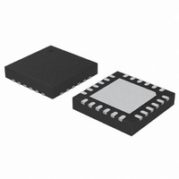
C8051F988-GM Silicon Laboratories Inc, C8051F988-GM Datasheet - Page 74

C8051F988-GM
Manufacturer Part Number
C8051F988-GM
Description
IC MCU 8BIT 4KB FLASH 24QFN
Manufacturer
Silicon Laboratories Inc
Series
C8051F9xxr
Specifications of C8051F988-GM
Program Memory Type
FLASH
Program Memory Size
4KB (4K x 8)
Package / Case
24-UQFN Exposed Pad, 24-HUQFN
Core Processor
8051
Core Size
8-Bit
Speed
25MHz
Connectivity
SMBus (2-Wire/I²C), SPI, UART/USART
Peripherals
Brown-out Detect/Reset, POR, PWM, Temp Sensor, WDT
Number Of I /o
17
Ram Size
512 x 8
Voltage - Supply (vcc/vdd)
1.8 V ~ 3.6 V
Data Converters
A/D 10x10b
Oscillator Type
Internal
Operating Temperature
-40°C ~ 85°C
Processor Series
C8051F9x
Core
8051
Data Ram Size
512 B
Interface Type
I2C, SMBus, Enhanced UART, Enhanced SPI
Maximum Clock Frequency
7 KHz
Number Of Programmable I/os
17
Number Of Timers
4
Operating Supply Voltage
2.4 V
Maximum Operating Temperature
+ 85 C
Mounting Style
SMD/SMT
3rd Party Development Tools
PK51, CA51, A51, ULINK2
Development Tools By Supplier
C8051F996DK
Minimum Operating Temperature
- 40 C
On-chip Adc
10 bit, 10 Channel
On-chip Dac
10 bit, 4 Channel
Lead Free Status / RoHS Status
Lead free / RoHS Compliant
Eeprom Size
-
Lead Free Status / Rohs Status
Lead free / RoHS Compliant
Other names
336-1959-5
- Current page: 74 of 322
- Download datasheet (3Mb)
C8051F99x-C8051F98x
SFR Definition 5.3. ADC0AC: ADC0 Accumulator Configuration
SFR Page = 0x0; SFR Address = 0xBA
74
Name AD012BE
Reset
Type
Bit
5:3
2:0
Bit
7
6
AD0SJST[2:0] ADC0 Accumulator Shift and Justify.
AD0RPT[2:0] ADC0 Repeat Count.
AD012BE
R/W
AD0AE
Name
7
0
AD0AE
ADC0 12-Bit Mode Enable.
Enables 12-bit Mode on C8051F980/6 and C8051F990/6 devices.
0: 12-bit Mode Disabled.
1: 12-bit Mode Enabled.
ADC0 Accumulate Enable.
Enables multiple conversions to be accumulated when burst mode is disabled.
0: ADC0H:ADC0L contain the result of the latest conversion when Burst Mode is
disabled.
1: ADC0H:ADC0L contain the accumulated conversion results when Burst Mode
is disabled. Software must write 0x0000 to ADC0H:ADC0L to clear the accumu-
lated result.
This bit is write-only. Always reads 0b.
Specifies the format of data read from ADC0H:ADC0L.
000: Right justified. No shifting applied.
001: Right justified. Shifted right by 1 bit.
010: Right justified. Shifted right by 2 bits.
011: Right justified. Shifted right by 3 bits.
100: Left justified. No shifting applied.
All remaining bit combinations are reserved.
Selects the number of conversions to perform and accumulate in Burst Mode.
This bit field must be set to 000 if Burst Mode is disabled.
000: Perform and Accumulate 1 conversion.
001: Perform and Accumulate 4 conversions.
010: Perform and Accumulate 8 conversions.
011: Perform and Accumulate 16 conversions.
100: Perform and Accumulate 32 conversions.
101: Perform and Accumulate 64 conversions.
All remaining bit combinations are reserved.
W
6
0
5
0
AD0SJST[2:0]
R/W
Rev. 1.0
4
0
Function
3
0
2
0
AD0RPT[2:0]
R/W
1
0
0
0
Related parts for C8051F988-GM
Image
Part Number
Description
Manufacturer
Datasheet
Request
R
Part Number:
Description:
SMD/C°/SINGLE-ENDED OUTPUT SILICON OSCILLATOR
Manufacturer:
Silicon Laboratories Inc
Part Number:
Description:
Manufacturer:
Silicon Laboratories Inc
Datasheet:
Part Number:
Description:
N/A N/A/SI4010 AES KEYFOB DEMO WITH LCD RX
Manufacturer:
Silicon Laboratories Inc
Datasheet:
Part Number:
Description:
N/A N/A/SI4010 SIMPLIFIED KEY FOB DEMO WITH LED RX
Manufacturer:
Silicon Laboratories Inc
Datasheet:
Part Number:
Description:
N/A/-40 TO 85 OC/EZLINK MODULE; F930/4432 HIGH BAND (REV E/B1)
Manufacturer:
Silicon Laboratories Inc
Part Number:
Description:
EZLink Module; F930/4432 Low Band (rev e/B1)
Manufacturer:
Silicon Laboratories Inc
Part Number:
Description:
I°/4460 10 DBM RADIO TEST CARD 434 MHZ
Manufacturer:
Silicon Laboratories Inc
Part Number:
Description:
I°/4461 14 DBM RADIO TEST CARD 868 MHZ
Manufacturer:
Silicon Laboratories Inc
Part Number:
Description:
I°/4463 20 DBM RFSWITCH RADIO TEST CARD 460 MHZ
Manufacturer:
Silicon Laboratories Inc
Part Number:
Description:
I°/4463 20 DBM RADIO TEST CARD 868 MHZ
Manufacturer:
Silicon Laboratories Inc
Part Number:
Description:
I°/4463 27 DBM RADIO TEST CARD 868 MHZ
Manufacturer:
Silicon Laboratories Inc
Part Number:
Description:
I°/4463 SKYWORKS 30 DBM RADIO TEST CARD 915 MHZ
Manufacturer:
Silicon Laboratories Inc
Part Number:
Description:
N/A N/A/-40 TO 85 OC/4463 RFMD 30 DBM RADIO TEST CARD 915 MHZ
Manufacturer:
Silicon Laboratories Inc
Part Number:
Description:
I°/4463 20 DBM RADIO TEST CARD 169 MHZ
Manufacturer:
Silicon Laboratories Inc


