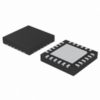
C8051F988-GM Silicon Laboratories Inc, C8051F988-GM Datasheet - Page 87

C8051F988-GM
Manufacturer Part Number
C8051F988-GM
Description
IC MCU 8BIT 4KB FLASH 24QFN
Manufacturer
Silicon Laboratories Inc
Series
C8051F9xxr
Specifications of C8051F988-GM
Program Memory Type
FLASH
Program Memory Size
4KB (4K x 8)
Package / Case
24-UQFN Exposed Pad, 24-HUQFN
Core Processor
8051
Core Size
8-Bit
Speed
25MHz
Connectivity
SMBus (2-Wire/I²C), SPI, UART/USART
Peripherals
Brown-out Detect/Reset, POR, PWM, Temp Sensor, WDT
Number Of I /o
17
Ram Size
512 x 8
Voltage - Supply (vcc/vdd)
1.8 V ~ 3.6 V
Data Converters
A/D 10x10b
Oscillator Type
Internal
Operating Temperature
-40°C ~ 85°C
Processor Series
C8051F9x
Core
8051
Data Ram Size
512 B
Interface Type
I2C, SMBus, Enhanced UART, Enhanced SPI
Maximum Clock Frequency
7 KHz
Number Of Programmable I/os
17
Number Of Timers
4
Operating Supply Voltage
2.4 V
Maximum Operating Temperature
+ 85 C
Mounting Style
SMD/SMT
3rd Party Development Tools
PK51, CA51, A51, ULINK2
Development Tools By Supplier
C8051F996DK
Minimum Operating Temperature
- 40 C
On-chip Adc
10 bit, 10 Channel
On-chip Dac
10 bit, 4 Channel
Lead Free Status / RoHS Status
Lead free / RoHS Compliant
Eeprom Size
-
Lead Free Status / Rohs Status
Lead free / RoHS Compliant
Other names
336-1959-5
- Current page: 87 of 322
- Download datasheet (3Mb)
C8051F99x-C8051F98x
5.10. External Voltage Reference
To use an external voltage reference, REFSL[1:0] should be set to 00. Bypass capacitors should be added
as recommended by the manufacturer of the external voltage reference. If the manufacturer does not pro-
vide recommendations, a 4.7uF in parallel with a 0.1uF capacitor is recommended.
5.11. Internal Voltage Reference
For applications requiring the maximum number of port I/O pins, or very short VREF turn-on time, the
1.65 V high-speed reference will be the best internal reference option to choose. The high speed internal
reference is selected by setting REFSL[1:0] to 11. When selected, the high speed internal reference will be
automatically enabled/disabled on an as-needed basis by ADC0.
For applications with a non-varying power supply voltage, using the power supply as the voltage reference
can provide ADC0 with added dynamic range at the cost of reduced power supply noise rejection. To use
the 1.8 to 3.6 V power supply voltage (V
) or the 1.8 V regulated digital supply voltage as the reference
DD
source, REFSL[1:0] should be set to 01 or 10, respectively.
5.12. Analog Ground Reference
To prevent ground noise generated by switching digital logic from affecting sensitive analog
measurements, a separate analog ground reference option is available. When enabled, the ground
reference for ADC0 during both the tracking/sampling and the conversion periods is taken from the
P0.1/AGND pin. Any external sensors sampled by ADC0 should be referenced to the P0.1/AGND pin. This
pin should be connected to the ground terminal of any external sensors sampled by ADC0. If an external
voltage reference is used, the P0.1/AGND pin should be connected to the ground of the external reference
and its associated decoupling capacitor. The separate analog ground reference option is enabled by
setting REFGND to 1. Note that when sampling the internal temperature sensor, the internal chip ground is
always used for the sampling operation, regardless of the setting of the REFGND bit. Similarly, whenever
the internal 1.65 V high-speed reference is selected, the internal chip ground is always used during the
conversion period, regardless of the setting of the REFGND bit.
5.13. Temperature Sensor Enable
The TEMPE bit in register REF0CN enables/disables the temperature sensor. While disabled, the
temperature sensor defaults to a high impedance state and any ADC0 measurements performed on the
sensor result in meaningless data. See Section “5.8. Temperature Sensor” on page 83 for details on
temperature sensor characteristics when it is enabled.
Rev. 1.0
87
Related parts for C8051F988-GM
Image
Part Number
Description
Manufacturer
Datasheet
Request
R
Part Number:
Description:
SMD/C°/SINGLE-ENDED OUTPUT SILICON OSCILLATOR
Manufacturer:
Silicon Laboratories Inc
Part Number:
Description:
Manufacturer:
Silicon Laboratories Inc
Datasheet:
Part Number:
Description:
N/A N/A/SI4010 AES KEYFOB DEMO WITH LCD RX
Manufacturer:
Silicon Laboratories Inc
Datasheet:
Part Number:
Description:
N/A N/A/SI4010 SIMPLIFIED KEY FOB DEMO WITH LED RX
Manufacturer:
Silicon Laboratories Inc
Datasheet:
Part Number:
Description:
N/A/-40 TO 85 OC/EZLINK MODULE; F930/4432 HIGH BAND (REV E/B1)
Manufacturer:
Silicon Laboratories Inc
Part Number:
Description:
EZLink Module; F930/4432 Low Band (rev e/B1)
Manufacturer:
Silicon Laboratories Inc
Part Number:
Description:
I°/4460 10 DBM RADIO TEST CARD 434 MHZ
Manufacturer:
Silicon Laboratories Inc
Part Number:
Description:
I°/4461 14 DBM RADIO TEST CARD 868 MHZ
Manufacturer:
Silicon Laboratories Inc
Part Number:
Description:
I°/4463 20 DBM RFSWITCH RADIO TEST CARD 460 MHZ
Manufacturer:
Silicon Laboratories Inc
Part Number:
Description:
I°/4463 20 DBM RADIO TEST CARD 868 MHZ
Manufacturer:
Silicon Laboratories Inc
Part Number:
Description:
I°/4463 27 DBM RADIO TEST CARD 868 MHZ
Manufacturer:
Silicon Laboratories Inc
Part Number:
Description:
I°/4463 SKYWORKS 30 DBM RADIO TEST CARD 915 MHZ
Manufacturer:
Silicon Laboratories Inc
Part Number:
Description:
N/A N/A/-40 TO 85 OC/4463 RFMD 30 DBM RADIO TEST CARD 915 MHZ
Manufacturer:
Silicon Laboratories Inc
Part Number:
Description:
I°/4463 20 DBM RADIO TEST CARD 169 MHZ
Manufacturer:
Silicon Laboratories Inc


