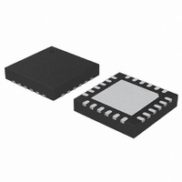
C8051F988-GM Silicon Laboratories Inc, C8051F988-GM Datasheet - Page 80

C8051F988-GM
Manufacturer Part Number
C8051F988-GM
Description
IC MCU 8BIT 4KB FLASH 24QFN
Manufacturer
Silicon Laboratories Inc
Series
C8051F9xxr
Specifications of C8051F988-GM
Program Memory Type
FLASH
Program Memory Size
4KB (4K x 8)
Package / Case
24-UQFN Exposed Pad, 24-HUQFN
Core Processor
8051
Core Size
8-Bit
Speed
25MHz
Connectivity
SMBus (2-Wire/I²C), SPI, UART/USART
Peripherals
Brown-out Detect/Reset, POR, PWM, Temp Sensor, WDT
Number Of I /o
17
Ram Size
512 x 8
Voltage - Supply (vcc/vdd)
1.8 V ~ 3.6 V
Data Converters
A/D 10x10b
Oscillator Type
Internal
Operating Temperature
-40°C ~ 85°C
Processor Series
C8051F9x
Core
8051
Data Ram Size
512 B
Interface Type
I2C, SMBus, Enhanced UART, Enhanced SPI
Maximum Clock Frequency
7 KHz
Number Of Programmable I/os
17
Number Of Timers
4
Operating Supply Voltage
2.4 V
Maximum Operating Temperature
+ 85 C
Mounting Style
SMD/SMT
3rd Party Development Tools
PK51, CA51, A51, ULINK2
Development Tools By Supplier
C8051F996DK
Minimum Operating Temperature
- 40 C
On-chip Adc
10 bit, 10 Channel
On-chip Dac
10 bit, 4 Channel
Lead Free Status / RoHS Status
Lead free / RoHS Compliant
Eeprom Size
-
Lead Free Status / Rohs Status
Lead free / RoHS Compliant
Other names
336-1959-5
- Current page: 80 of 322
- Download datasheet (3Mb)
C8051F99x-C8051F98x
5.6.1. Window Detector In Single-Ended Mode
Figure 5.5
ADC0LTH:ADC0LTL = 0x0080 (128d) and ADC0GTH:ADC0GTL = 0x0040 (64d). The input voltage can
range from 0 to VREF x (1023/1024) with respect to GND, and is represented by a 10-bit unsigned integer
value. In the left example, an AD0WINT interrupt will be generated if the ADC0 conversion word
(ADC0H:ADC0L) is within the range defined by ADC0GTH:ADC0GTL and ADC0LTH:ADC0LTL
(if 0x0040 < ADC0H:ADC0L < 0x0080). In the right example, and AD0WINT interrupt will be generated if
the ADC0 conversion word is outside of the range defined by the ADC0GT and ADC0LT registers
(if ADC0H:ADC0L < 0x0040 or ADC0H:ADC0L > 0x0080). Figure 5.6 shows an example using left-
justified data with the same comparison values.
5.6.2. ADC0 Specifications
See “4. Electrical Characteristics” on page 46 for a detailed listing of ADC0 specifications.
80
VREF x (1023/1024)
VREF x (1023/1024)
VREF x (128/1024)
VREF x (128/1024)
VREF x (64/1024)
VREF x (64/1024)
Input Voltage
(Px.x - GND)
Input Voltage
(Px.x - GND)
Figure 5.5. ADC Window Compare Example: Right-Justified Single-Ended Data
Figure 5.6. ADC Window Compare Example: Left-Justified Single-Ended Data
0
0
shows
ADC0H:ADC0L
ADC0H:ADC0L
0xFFC0
0x1FC0
0x0FC0
0x2040
0x2000
0x1040
0x1000
0x0000
0x03FF
0x0081
0x0080
0x007F
0x0041
0x0040
0x003F
0x0000
two
example
ADC0GTH:ADC0GTL
ADC0GTH:ADC0GTL
ADC0LTH:ADC0LTL
ADC0LTH:ADC0LTL
not affected
not affected
not affected
not affected
AD0WINT
AD0WINT
AD0WINT
AD0WINT
AD0WINT=1
AD0WINT=1
window
Rev. 1.0
VREF x (1023/1024)
VREF x (1023/1024)
VREF x (128/1024)
VREF x (128/1024)
comparisons
VREF x (64/1024)
VREF x (64/1024)
Input Voltage
Input Voltage
(Px.x - GND)
(Px.x - GND)
0
0
ADC0H:ADC0L
ADC0H:ADC0L
0x03FF
0xFFC0
0x1FC0
0x0FC0
0x0081
0x0080
0x007F
0x0041
0x0040
0x003F
0x0000
0x2040
0x2000
0x1040
0x1000
0x0000
for
right-justified
ADC0GTH:ADC0GTL
ADC0GTH:ADC0GTL
ADC0LTH:ADC0LTL
ADC0LTH:ADC0LTL
not affected
not affected
AD0WINT
AD0WINT
data,
AD0WINT=1
AD0WINT=1
AD0WINT=1
AD0WINT=1
with
Related parts for C8051F988-GM
Image
Part Number
Description
Manufacturer
Datasheet
Request
R
Part Number:
Description:
SMD/C°/SINGLE-ENDED OUTPUT SILICON OSCILLATOR
Manufacturer:
Silicon Laboratories Inc
Part Number:
Description:
Manufacturer:
Silicon Laboratories Inc
Datasheet:
Part Number:
Description:
N/A N/A/SI4010 AES KEYFOB DEMO WITH LCD RX
Manufacturer:
Silicon Laboratories Inc
Datasheet:
Part Number:
Description:
N/A N/A/SI4010 SIMPLIFIED KEY FOB DEMO WITH LED RX
Manufacturer:
Silicon Laboratories Inc
Datasheet:
Part Number:
Description:
N/A/-40 TO 85 OC/EZLINK MODULE; F930/4432 HIGH BAND (REV E/B1)
Manufacturer:
Silicon Laboratories Inc
Part Number:
Description:
EZLink Module; F930/4432 Low Band (rev e/B1)
Manufacturer:
Silicon Laboratories Inc
Part Number:
Description:
I°/4460 10 DBM RADIO TEST CARD 434 MHZ
Manufacturer:
Silicon Laboratories Inc
Part Number:
Description:
I°/4461 14 DBM RADIO TEST CARD 868 MHZ
Manufacturer:
Silicon Laboratories Inc
Part Number:
Description:
I°/4463 20 DBM RFSWITCH RADIO TEST CARD 460 MHZ
Manufacturer:
Silicon Laboratories Inc
Part Number:
Description:
I°/4463 20 DBM RADIO TEST CARD 868 MHZ
Manufacturer:
Silicon Laboratories Inc
Part Number:
Description:
I°/4463 27 DBM RADIO TEST CARD 868 MHZ
Manufacturer:
Silicon Laboratories Inc
Part Number:
Description:
I°/4463 SKYWORKS 30 DBM RADIO TEST CARD 915 MHZ
Manufacturer:
Silicon Laboratories Inc
Part Number:
Description:
N/A N/A/-40 TO 85 OC/4463 RFMD 30 DBM RADIO TEST CARD 915 MHZ
Manufacturer:
Silicon Laboratories Inc
Part Number:
Description:
I°/4463 20 DBM RADIO TEST CARD 169 MHZ
Manufacturer:
Silicon Laboratories Inc


