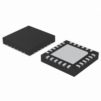
C8051F988-GM Silicon Laboratories Inc, C8051F988-GM Datasheet - Page 34

C8051F988-GM
Manufacturer Part Number
C8051F988-GM
Description
IC MCU 8BIT 4KB FLASH 24QFN
Manufacturer
Silicon Laboratories Inc
Series
C8051F9xxr
Specifications of C8051F988-GM
Program Memory Type
FLASH
Program Memory Size
4KB (4K x 8)
Package / Case
24-UQFN Exposed Pad, 24-HUQFN
Core Processor
8051
Core Size
8-Bit
Speed
25MHz
Connectivity
SMBus (2-Wire/I²C), SPI, UART/USART
Peripherals
Brown-out Detect/Reset, POR, PWM, Temp Sensor, WDT
Number Of I /o
17
Ram Size
512 x 8
Voltage - Supply (vcc/vdd)
1.8 V ~ 3.6 V
Data Converters
A/D 10x10b
Oscillator Type
Internal
Operating Temperature
-40°C ~ 85°C
Processor Series
C8051F9x
Core
8051
Data Ram Size
512 B
Interface Type
I2C, SMBus, Enhanced UART, Enhanced SPI
Maximum Clock Frequency
7 KHz
Number Of Programmable I/os
17
Number Of Timers
4
Operating Supply Voltage
2.4 V
Maximum Operating Temperature
+ 85 C
Mounting Style
SMD/SMT
3rd Party Development Tools
PK51, CA51, A51, ULINK2
Development Tools By Supplier
C8051F996DK
Minimum Operating Temperature
- 40 C
On-chip Adc
10 bit, 10 Channel
On-chip Dac
10 bit, 4 Channel
Lead Free Status / RoHS Status
Lead free / RoHS Compliant
Eeprom Size
-
Lead Free Status / Rohs Status
Lead free / RoHS Compliant
Other names
336-1959-5
- Current page: 34 of 322
- Download datasheet (3Mb)
C8051F99x-C8051F98x
34
*Note: Available only on the C8051F980/2/6/8 and C8051F990/6 devices.
CNVSTR*
IREF0
Name
CP0+
P0.6/
P0.7/
CP0-
P1.0
P1.1
P1.2
P1.3
P1.4
P1.5
Table 3.1. Pin Definitions for the C8051F99x-C8051F98x (Continued)
‘F980/1/2
‘F983/5
‘F990/1
-GM
16
15
14
13
10
11
—
9
Pin Numbers
‘F986/7
‘F988/9
‘F996/7
-GM
18
17
16
15
14
13
12
11
‘F986/7
‘F988/9
‘F996/7
-GU
21
20
19
18
17
16
15
14
D I/O or
D I/O or
D I/O or
D I/O or
D I/O or
D I/O or
D I/O or
D I/O or
A Out
Type
D In
A In
A In
A In
A In
A In
A In
A In
A In
A In
A In
Rev. 1.0
Description
Port 0.6. See Section “21. Port Input/Output” on
page 213 for a complete description.
External Convert Start Input for ADC0. See Section
“5.7. ADC0 Analog Multiplexer” on page 81 for a
complete description.
Port 0.7. See Section “21. Port Input/Output” on
page 213 for a complete description.
IREF0 Output. See IREF Section for complete
description.
Port 1.0. See Section “21. Port Input/Output” on
page 213 for a complete description. May also be used
as SCK for SPI1.
Comparator0 positive input. See Comparator Section for
complete description.
Port 1.1. See Section “21. Port Input/Output” on
page 213 for a complete description.
Comparator0 negative input. See Comparator Section
for complete description.
Port 1.2. See Section “21. Port Input/Output” on
page 213 for a complete description.
Port 1.3. See Section “21. Port Input/Output” on
page 213 for a complete description.
Port 1.4. See Section “21. Port Input/Output” on
page 213 for a complete description.
Port 1.5. See Section “21. Port Input/Output” on
page 213 for a complete description.
Related parts for C8051F988-GM
Image
Part Number
Description
Manufacturer
Datasheet
Request
R
Part Number:
Description:
SMD/C°/SINGLE-ENDED OUTPUT SILICON OSCILLATOR
Manufacturer:
Silicon Laboratories Inc
Part Number:
Description:
Manufacturer:
Silicon Laboratories Inc
Datasheet:
Part Number:
Description:
N/A N/A/SI4010 AES KEYFOB DEMO WITH LCD RX
Manufacturer:
Silicon Laboratories Inc
Datasheet:
Part Number:
Description:
N/A N/A/SI4010 SIMPLIFIED KEY FOB DEMO WITH LED RX
Manufacturer:
Silicon Laboratories Inc
Datasheet:
Part Number:
Description:
N/A/-40 TO 85 OC/EZLINK MODULE; F930/4432 HIGH BAND (REV E/B1)
Manufacturer:
Silicon Laboratories Inc
Part Number:
Description:
EZLink Module; F930/4432 Low Band (rev e/B1)
Manufacturer:
Silicon Laboratories Inc
Part Number:
Description:
I°/4460 10 DBM RADIO TEST CARD 434 MHZ
Manufacturer:
Silicon Laboratories Inc
Part Number:
Description:
I°/4461 14 DBM RADIO TEST CARD 868 MHZ
Manufacturer:
Silicon Laboratories Inc
Part Number:
Description:
I°/4463 20 DBM RFSWITCH RADIO TEST CARD 460 MHZ
Manufacturer:
Silicon Laboratories Inc
Part Number:
Description:
I°/4463 20 DBM RADIO TEST CARD 868 MHZ
Manufacturer:
Silicon Laboratories Inc
Part Number:
Description:
I°/4463 27 DBM RADIO TEST CARD 868 MHZ
Manufacturer:
Silicon Laboratories Inc
Part Number:
Description:
I°/4463 SKYWORKS 30 DBM RADIO TEST CARD 915 MHZ
Manufacturer:
Silicon Laboratories Inc
Part Number:
Description:
N/A N/A/-40 TO 85 OC/4463 RFMD 30 DBM RADIO TEST CARD 915 MHZ
Manufacturer:
Silicon Laboratories Inc
Part Number:
Description:
I°/4463 20 DBM RADIO TEST CARD 169 MHZ
Manufacturer:
Silicon Laboratories Inc


