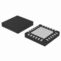
C8051F988-GM Silicon Laboratories Inc, C8051F988-GM Datasheet - Page 304

C8051F988-GM
Manufacturer Part Number
C8051F988-GM
Description
IC MCU 8BIT 4KB FLASH 24QFN
Manufacturer
Silicon Laboratories Inc
Series
C8051F9xxr
Specifications of C8051F988-GM
Program Memory Type
FLASH
Program Memory Size
4KB (4K x 8)
Package / Case
24-UQFN Exposed Pad, 24-HUQFN
Core Processor
8051
Core Size
8-Bit
Speed
25MHz
Connectivity
SMBus (2-Wire/I²C), SPI, UART/USART
Peripherals
Brown-out Detect/Reset, POR, PWM, Temp Sensor, WDT
Number Of I /o
17
Ram Size
512 x 8
Voltage - Supply (vcc/vdd)
1.8 V ~ 3.6 V
Data Converters
A/D 10x10b
Oscillator Type
Internal
Operating Temperature
-40°C ~ 85°C
Processor Series
C8051F9x
Core
8051
Data Ram Size
512 B
Interface Type
I2C, SMBus, Enhanced UART, Enhanced SPI
Maximum Clock Frequency
7 KHz
Number Of Programmable I/os
17
Number Of Timers
4
Operating Supply Voltage
2.4 V
Maximum Operating Temperature
+ 85 C
Mounting Style
SMD/SMT
3rd Party Development Tools
PK51, CA51, A51, ULINK2
Development Tools By Supplier
C8051F996DK
Minimum Operating Temperature
- 40 C
On-chip Adc
10 bit, 10 Channel
On-chip Dac
10 bit, 4 Channel
Lead Free Status / RoHS Status
Lead free / RoHS Compliant
Eeprom Size
-
Lead Free Status / Rohs Status
Lead free / RoHS Compliant
Other names
336-1959-5
- Current page: 304 of 322
- Download datasheet (3Mb)
C8051F99x-C8051F98x
26.3.3. High-Speed Output Mode
In High-Speed Output mode, a module’s associated CEXn pin is toggled each time a match occurs
between the PCA Counter and the module's 16-bit capture/compare register (PCA0CPHn and
PCA0CPLn). When a match occurs, the Capture/Compare Flag (CCFn) in PCA0CN is set to logic 1. An
interrupt request is generated if the CCFn interrupt for that module is enabled. The CCFn bit is not
automatically cleared by hardware when the CPU vectors to the interrupt service routine, and must be
cleared by software. Setting the TOGn, MATn, and ECOMn bits in the PCA0CPMn register enables the
High-Speed Output mode. If ECOMn is cleared, the associated pin will retain its state, and not toggle on
the next match event.
Important Note About Capture/Compare Registers: When writing a 16-bit value to the PCA0
Capture/Compare registers, the low byte should always be written first. Writing to PCA0CPLn clears the
ECOMn bit to 0; writing to PCA0CPHn sets ECOMn to 1.
26.3.4. Frequency Output Mode
Frequency Output Mode produces a programmable-frequency square wave on the module’s associated
CEXn pin. The capture/compare module high byte holds the number of PCA clocks to count before the
output is toggled. The frequency of the square wave is then defined by Equation 26.1.
304
Note: A value of 0x00 in the PCA0CPHn register is equal to 256 for this equation.
PCA0CPLn
Write to
Reset
PCA0CPHn
Write to
0
ENB
ENB
1
PCA
Timebase
Figure 26.6. PCA High-Speed Output Mode Diagram
Enable
Equation 26.1. Square Wave Frequency Output
P
W
M
1
6
n
x
C
O
M
E
n
PCA0CPLn
PCA0CPMn
C
A
P
P
n
0 0
PCA0L
C
N
A
P
n
16-bit Comparator
M
A
T
n
O
G
T
n
F
W
M
P
n
0 x
CEXn
E
C
C
F
n
PCA0CPHn
PCA0H
=
---------------------------------------- -
2
Rev. 1.0
PCA0CPHn
F
PCA
Match
Toggle
C
F
C
R
TOGn
0
1
PCA0CN
0
1
CEXn
C
C
F
2
C
C
F
1
C
C
F
0
PCA Interrupt
Crossbar
Port I/O
Related parts for C8051F988-GM
Image
Part Number
Description
Manufacturer
Datasheet
Request
R
Part Number:
Description:
SMD/C°/SINGLE-ENDED OUTPUT SILICON OSCILLATOR
Manufacturer:
Silicon Laboratories Inc
Part Number:
Description:
Manufacturer:
Silicon Laboratories Inc
Datasheet:
Part Number:
Description:
N/A N/A/SI4010 AES KEYFOB DEMO WITH LCD RX
Manufacturer:
Silicon Laboratories Inc
Datasheet:
Part Number:
Description:
N/A N/A/SI4010 SIMPLIFIED KEY FOB DEMO WITH LED RX
Manufacturer:
Silicon Laboratories Inc
Datasheet:
Part Number:
Description:
N/A/-40 TO 85 OC/EZLINK MODULE; F930/4432 HIGH BAND (REV E/B1)
Manufacturer:
Silicon Laboratories Inc
Part Number:
Description:
EZLink Module; F930/4432 Low Band (rev e/B1)
Manufacturer:
Silicon Laboratories Inc
Part Number:
Description:
I°/4460 10 DBM RADIO TEST CARD 434 MHZ
Manufacturer:
Silicon Laboratories Inc
Part Number:
Description:
I°/4461 14 DBM RADIO TEST CARD 868 MHZ
Manufacturer:
Silicon Laboratories Inc
Part Number:
Description:
I°/4463 20 DBM RFSWITCH RADIO TEST CARD 460 MHZ
Manufacturer:
Silicon Laboratories Inc
Part Number:
Description:
I°/4463 20 DBM RADIO TEST CARD 868 MHZ
Manufacturer:
Silicon Laboratories Inc
Part Number:
Description:
I°/4463 27 DBM RADIO TEST CARD 868 MHZ
Manufacturer:
Silicon Laboratories Inc
Part Number:
Description:
I°/4463 SKYWORKS 30 DBM RADIO TEST CARD 915 MHZ
Manufacturer:
Silicon Laboratories Inc
Part Number:
Description:
N/A N/A/-40 TO 85 OC/4463 RFMD 30 DBM RADIO TEST CARD 915 MHZ
Manufacturer:
Silicon Laboratories Inc
Part Number:
Description:
I°/4463 20 DBM RADIO TEST CARD 169 MHZ
Manufacturer:
Silicon Laboratories Inc


