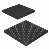
AT91SAM9263B-CU Atmel, AT91SAM9263B-CU Datasheet - Page 238

AT91SAM9263B-CU
Manufacturer Part Number
AT91SAM9263B-CU
Description
IC ARM9 MCU 200 MHZ 324-TFBGA
Manufacturer
Atmel
Series
AT91SAMr
Specifications of AT91SAM9263B-CU
Core Processor
ARM9
Core Size
16/32-Bit
Speed
240MHz
Connectivity
CAN, Ethernet, I²C, MMC, SPI, SSC, UART/USART, USB
Peripherals
AC'97, LCD, POR, PWM, WDT
Number Of I /o
160
Program Memory Size
128KB (128K x 8)
Program Memory Type
ROM
Ram Size
128K x 8
Voltage - Supply (vcc/vdd)
1.08 V ~ 1.32 V
Oscillator Type
Internal
Operating Temperature
-40°C ~ 85°C
Package / Case
324-TFBGA
Processor Series
AT91SAMx
Core
ARM926EJ-S
Data Bus Width
32 bit
Data Ram Size
96 KB
Interface Type
2-Wire, EBI, I2S, MCI, SPI, USART
Maximum Clock Frequency
200 MHz
Number Of Programmable I/os
160
Number Of Timers
4
Maximum Operating Temperature
+ 85 C
Mounting Style
SMD/SMT
3rd Party Development Tools
JTRACE-ARM-2M, MDK-ARM, RL-ARM, ULINK2
Development Tools By Supplier
AT91SAM-ICE, AT91-ISP, AT91SAM9263-EK
Minimum Operating Temperature
- 40 C
Package
324TFBGA
Device Core
ARM926EJ-S
Family Name
91S
Maximum Speed
200 MHz
Operating Supply Voltage
1.8|2.5|3.3 V
Controller Family/series
AT91SAM9xxx
No. Of I/o's
160
Ram Memory Size
96KB
Cpu Speed
240MHz
No. Of Timers
1
Rohs Compliant
Yes
For Use With
AT91SAM9263-EK - KIT EVAL FOR AT91SAM9263AT91SAM-ICE - EMULATOR FOR AT91 ARM7/ARM9
Lead Free Status / RoHS Status
Lead free / RoHS Compliant
Eeprom Size
-
Data Converters
-
Lead Free Status / Rohs Status
Lead free / RoHS Compliant
Other names
Q3735625
Available stocks
Company
Part Number
Manufacturer
Quantity
Price
Company:
Part Number:
AT91SAM9263B-CU
Manufacturer:
IDT
Quantity:
1 043
Part Number:
AT91SAM9263B-CU
Manufacturer:
ATMEL/爱特梅尔
Quantity:
20 000
Company:
Part Number:
AT91SAM9263B-CU-100
Manufacturer:
ATMEL
Quantity:
1 000
- Current page: 238 of 1110
- Download datasheet (17Mb)
23.5
23.5.1
Figure 23-2. Write Burst, 32-bit SDRAM Access
SDRAMC_A[12:0]
23.5.2
6249H–ATARM–27-Jul-09
D[31:0]
SDWE
SDCS
SDCK
Functional Description
RAS
CAS
SDRAM Controller Write Cycle
SDRAM Controller Read Cycle
Row n
The SDRAM Controller allows burst access or single access. In both cases, the SDRAM control-
ler keeps track of the active row in each bank, thus maximizing performance. To initiate a burst
access, the SDRAM Controller uses the transfer type signal provided by the master requesting
the access. If the next access is a sequential write access, writing to the SDRAM device is car-
ried out. If the next access is a write-sequential access, but the current access is to a boundary
page, or if the next access is in another row, then the SDRAM Controller generates a precharge
command, activates the new row and initiates a write command. To comply with SDRAM timing
parameters, additional clock cycles are inserted between precharge/active (t
active/write (t
Configuration Register” on page
The SDRAM Controller allows burst access, incremental burst of unspecified length or single
access. In all cases, the SDRAM Controller keeps track of the active row in each bank, thus
maximizing performance of the SDRAM. If row and bank addresses do not match the previous
row/bank address, then the SDRAM controller automatically generates a precharge command,
activates the new row and starts the read command. To comply with the SDRAM timing param-
eters, additional clock cycles on SDCK are inserted between precharge and active commands
(t
uration register of the SDRAM Controller. After a read command, additional wait states are
generated to comply with the CAS latency (1, 2 or 3 clock delays specified in the configuration
register).
RP
) and between active and read command (t
t
RCD
= 3
col a
RCD
Dna
) commands. For definition of these timing parameters, refer to the
col b
Dnb
col c
Dnc
249. This is described in
col d
Dnd
col e
Dne
RCD
col f
Dnf
). These two parameters are set in the config-
col g
Dng
Figure 23-2
col h
Dnh
AT91SAM9263
col i
Dni
below.
col j
Dnj
RP
) commands and
col k
Dnk
“SDRAMC
col l
Dnl
238
Related parts for AT91SAM9263B-CU
Image
Part Number
Description
Manufacturer
Datasheet
Request
R

Part Number:
Description:
MCU, MPU & DSP Development Tools KICKSTART KIT FOR AT91SAM9 PLUS
Manufacturer:
IAR Systems

Part Number:
Description:
DEV KIT FOR AVR/AVR32
Manufacturer:
Atmel
Datasheet:

Part Number:
Description:
INTERVAL AND WIPE/WASH WIPER CONTROL IC WITH DELAY
Manufacturer:
ATMEL Corporation
Datasheet:

Part Number:
Description:
Low-Voltage Voice-Switched IC for Hands-Free Operation
Manufacturer:
ATMEL Corporation
Datasheet:

Part Number:
Description:
MONOLITHIC INTEGRATED FEATUREPHONE CIRCUIT
Manufacturer:
ATMEL Corporation
Datasheet:

Part Number:
Description:
AM-FM Receiver IC U4255BM-M
Manufacturer:
ATMEL Corporation
Datasheet:

Part Number:
Description:
Monolithic Integrated Feature Phone Circuit
Manufacturer:
ATMEL Corporation
Datasheet:

Part Number:
Description:
Multistandard Video-IF and Quasi Parallel Sound Processing
Manufacturer:
ATMEL Corporation
Datasheet:

Part Number:
Description:
High-performance EE PLD
Manufacturer:
ATMEL Corporation
Datasheet:

Part Number:
Description:
8-bit Flash Microcontroller
Manufacturer:
ATMEL Corporation
Datasheet:

Part Number:
Description:
2-Wire Serial EEPROM
Manufacturer:
ATMEL Corporation
Datasheet:


