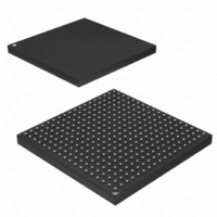
AT91SAM9263B-CU Atmel, AT91SAM9263B-CU Datasheet - Page 60

AT91SAM9263B-CU
Manufacturer Part Number
AT91SAM9263B-CU
Description
IC ARM9 MCU 200 MHZ 324-TFBGA
Manufacturer
Atmel
Series
AT91SAMr
Specifications of AT91SAM9263B-CU
Core Processor
ARM9
Core Size
16/32-Bit
Speed
240MHz
Connectivity
CAN, Ethernet, I²C, MMC, SPI, SSC, UART/USART, USB
Peripherals
AC'97, LCD, POR, PWM, WDT
Number Of I /o
160
Program Memory Size
128KB (128K x 8)
Program Memory Type
ROM
Ram Size
128K x 8
Voltage - Supply (vcc/vdd)
1.08 V ~ 1.32 V
Oscillator Type
Internal
Operating Temperature
-40°C ~ 85°C
Package / Case
324-TFBGA
Processor Series
AT91SAMx
Core
ARM926EJ-S
Data Bus Width
32 bit
Data Ram Size
96 KB
Interface Type
2-Wire, EBI, I2S, MCI, SPI, USART
Maximum Clock Frequency
200 MHz
Number Of Programmable I/os
160
Number Of Timers
4
Maximum Operating Temperature
+ 85 C
Mounting Style
SMD/SMT
3rd Party Development Tools
JTRACE-ARM-2M, MDK-ARM, RL-ARM, ULINK2
Development Tools By Supplier
AT91SAM-ICE, AT91-ISP, AT91SAM9263-EK
Minimum Operating Temperature
- 40 C
Package
324TFBGA
Device Core
ARM926EJ-S
Family Name
91S
Maximum Speed
200 MHz
Operating Supply Voltage
1.8|2.5|3.3 V
Controller Family/series
AT91SAM9xxx
No. Of I/o's
160
Ram Memory Size
96KB
Cpu Speed
240MHz
No. Of Timers
1
Rohs Compliant
Yes
For Use With
AT91SAM9263-EK - KIT EVAL FOR AT91SAM9263AT91SAM-ICE - EMULATOR FOR AT91 ARM7/ARM9
Lead Free Status / RoHS Status
Lead free / RoHS Compliant
Eeprom Size
-
Data Converters
-
Lead Free Status / Rohs Status
Lead free / RoHS Compliant
Other names
Q3735625
Available stocks
Company
Part Number
Manufacturer
Quantity
Price
Company:
Part Number:
AT91SAM9263B-CU
Manufacturer:
IDT
Quantity:
1 043
Part Number:
AT91SAM9263B-CU
Manufacturer:
ATMEL/爱特梅尔
Quantity:
20 000
Company:
Part Number:
AT91SAM9263B-CU-100
Manufacturer:
ATMEL
Quantity:
1 000
- Current page: 60 of 1110
- Download datasheet (17Mb)
11.5.2
11.5.3
11.5.4
11.6
60
Caches and Write Buffer
AT91SAM9263
Translation Look-aside Buffer (TLB)
Translation Table Walk Hardware
MMU Faults
The Translation Look-aside Buffer (TLB) caches translated entries and thus avoids going
through the translation process every time. When the TLB contains an entry for the MVA (Modi-
fied Virtual Address), the access control logic determines if the access is permitted and outputs
the appropriate physical address corresponding to the MVA. If access is not permitted, the MMU
signals the CPU core to abort.
If the TLB does not contain an entry for the MVA, the translation table walk hardware is invoked
to retrieve the translation information from the translation table in physical memory.
The translation table walk hardware is a logic that traverses the translation tables located in
physical memory, gets the physical address and access permissions and updates the TLB.
The number of stages in the hardware table walking is one or two depending whether the
address is marked as a section-mapped access or a page-mapped access.
There are three sizes of page-mapped accesses and one size of section-mapped access. Page-
mapped accesses are for large pages, small pages and tiny pages. The translation process
always begins with a level one fetch. A section-mapped access requires only a level one fetch,
but a page-mapped access requires an additional level two fetch. For further details on the
MMU, please refer to chapter 3 in ARM926EJ-S Technical Reference Manual, ref. DDI0198B.
The MMU generates an abort on the following types of faults:
The access control mechanism of the MMU detects the conditions that produce these faults. If
the fault is a result of memory access, the MMU aborts the access and signals the fault to the
CPU core.The MMU retains status and address information about faults generated by the data
accesses in the data fault status register and fault address register. It also retains the status of
faults generated by instruction fetches in the instruction fault status register.
The fault status register (register 5 in CP15) indicates the cause of a data or prefetch abort, and
the domain number of the aborted access when it happens. The fault address register (register 6
in CP15) holds the MVA associated with the access that caused the Data Abort. For further
details on MMU faults, please refer to chapter 3 in ARM926EJ-S Technical Reference Manual,
ref. DDI0198B.
The ARM926EJ-S contains a 16 KB Instruction Cache (ICache), a 16 KB Data Cache (DCache),
and a write buffer. Although the ICache and DCache share common features, each still has
some specific mechanisms.
The caches (ICache and DCache) are four-way set associative, addressed, indexed and tagged
using the Modified Virtual Address (MVA), with a cache line length of eight words with two dirty
bits for the DCache. The ICache and DCache provide mechanisms for cache lockdown, cache
pollution control, and line replacement.
• Alignment faults (for data accesses only)
• Translation faults
• Domain faults
• Permission faults
6249H–ATARM–27-Jul-09
Related parts for AT91SAM9263B-CU
Image
Part Number
Description
Manufacturer
Datasheet
Request
R

Part Number:
Description:
MCU, MPU & DSP Development Tools KICKSTART KIT FOR AT91SAM9 PLUS
Manufacturer:
IAR Systems

Part Number:
Description:
DEV KIT FOR AVR/AVR32
Manufacturer:
Atmel
Datasheet:

Part Number:
Description:
INTERVAL AND WIPE/WASH WIPER CONTROL IC WITH DELAY
Manufacturer:
ATMEL Corporation
Datasheet:

Part Number:
Description:
Low-Voltage Voice-Switched IC for Hands-Free Operation
Manufacturer:
ATMEL Corporation
Datasheet:

Part Number:
Description:
MONOLITHIC INTEGRATED FEATUREPHONE CIRCUIT
Manufacturer:
ATMEL Corporation
Datasheet:

Part Number:
Description:
AM-FM Receiver IC U4255BM-M
Manufacturer:
ATMEL Corporation
Datasheet:

Part Number:
Description:
Monolithic Integrated Feature Phone Circuit
Manufacturer:
ATMEL Corporation
Datasheet:

Part Number:
Description:
Multistandard Video-IF and Quasi Parallel Sound Processing
Manufacturer:
ATMEL Corporation
Datasheet:

Part Number:
Description:
High-performance EE PLD
Manufacturer:
ATMEL Corporation
Datasheet:

Part Number:
Description:
8-bit Flash Microcontroller
Manufacturer:
ATMEL Corporation
Datasheet:

Part Number:
Description:
2-Wire Serial EEPROM
Manufacturer:
ATMEL Corporation
Datasheet:


