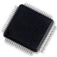
S9S12HY64J0MLH Freescale Semiconductor, S9S12HY64J0MLH Datasheet - Page 127

S9S12HY64J0MLH
Manufacturer Part Number
S9S12HY64J0MLH
Description
MCU 64K FLASH AUTO 64-LQFP
Manufacturer
Freescale Semiconductor
Series
HCS12r
Datasheet
1.S9S12HA32J0CLL.pdf
(792 pages)
Specifications of S9S12HY64J0MLH
Core Processor
HCS12
Core Size
16-Bit
Speed
32MHz
Connectivity
CAN, EBI/EMI, I²C, IrDA, LIN, SCI, SPI
Peripherals
LCD, Motor control PWM, POR, PWM, WDT
Number Of I /o
50
Program Memory Size
64KB (64K x 8)
Program Memory Type
FLASH
Eeprom Size
4K x 8
Ram Size
4K x 8
Voltage - Supply (vcc/vdd)
4.5 V ~ 5.5 V
Data Converters
A/D 6x10b
Oscillator Type
Internal
Operating Temperature
-40°C ~ 125°C
Package / Case
64-LQFP
Controller Family/series
S12
No. Of I/o's
50
Ram Memory Size
4KB
Cpu Speed
64MHz
No. Of Timers
2
Rohs Compliant
Yes
Processor Series
S12HY
Core
HCS12
3rd Party Development Tools
EWHCS12
Development Tools By Supplier
DEMO9S12HY64
Lead Free Status / RoHS Status
Lead free / RoHS Compliant
Available stocks
Company
Part Number
Manufacturer
Quantity
Price
Company:
Part Number:
S9S12HY64J0MLH
Manufacturer:
Freescale Semiconductor
Quantity:
10 000
- Current page: 127 of 792
- Download datasheet (4Mb)
1
2
1
1
2.3.87
2.3.88
2.4
2.4.1
Each pin except BKGD can act as general purpose I/O. In addition each pin can act as an output or input
of a peripheral module.
Freescale Semiconductor
Address 0x029E
Address 0x029F
When change SRRV from non-zero value to zero value or vice versa, It will need to wait about 300 nanoseconds delay before
the slew rate control to be real function as setting. When enter STOP, to save the power, the slew rate control will be force to off
state. After wakeup from STOP, it will also need to wait about 300 nanoseconds before slew rate control to be function as setting.
When MC function is disabled and IIC/SPI/PWM async shutdown are routing to PV and enabled, the corresponding digital input
buffer will be always enabled
Read: Anytime.
Write: Anytime.
Read: Always reads 0x00
Write: Unimplemented
SRRV
Field
Reset
Reset
7-0
W
W
R
R
Functional Description
Port V Slew Rate Register—Determine the slew rate on the pins
1 Enable the slew rate control and disables the digital input buffer
0 Disable the slew rate control and enable the digital input buffer
SRRV7
Port V Slew Rate Register(SRRV)
PIM Reserved Registers
General
0
0
0
7
7
= Unimplemented or Reserved
SRRV6
0
0
0
6
6
Figure 2-85. Port V Polarity Select Register (SRRV)
MC9S12HY/HA-Family Reference Manual, Rev. 1.04
Table 2-73. SRRV Register Field Descriptions
Figure 2-86. PIM Reserved Registers
SRRV5
0
0
0
5
5
SRRV4
0
0
0
4
4
Description
u = Unaffected by reset
SRRV3
3
0
3
0
0
2
1
SRRV2
Port Integration Module (S12HYPIMV1)
0
0
0
2
2
SRRV1
Access: User read/write
0
0
0
1
1
Access: User read
SRRV0
0
0
0
0
0
127
1
1
Related parts for S9S12HY64J0MLH
Image
Part Number
Description
Manufacturer
Datasheet
Request
R
Part Number:
Description:
Manufacturer:
Freescale Semiconductor, Inc
Datasheet:
Part Number:
Description:
Manufacturer:
Freescale Semiconductor, Inc
Datasheet:
Part Number:
Description:
Manufacturer:
Freescale Semiconductor, Inc
Datasheet:
Part Number:
Description:
Manufacturer:
Freescale Semiconductor, Inc
Datasheet:
Part Number:
Description:
Manufacturer:
Freescale Semiconductor, Inc
Datasheet:
Part Number:
Description:
Manufacturer:
Freescale Semiconductor, Inc
Datasheet:
Part Number:
Description:
Manufacturer:
Freescale Semiconductor, Inc
Datasheet:
Part Number:
Description:
Manufacturer:
Freescale Semiconductor, Inc
Datasheet:
Part Number:
Description:
Manufacturer:
Freescale Semiconductor, Inc
Datasheet:
Part Number:
Description:
Manufacturer:
Freescale Semiconductor, Inc
Datasheet:
Part Number:
Description:
Manufacturer:
Freescale Semiconductor, Inc
Datasheet:
Part Number:
Description:
Manufacturer:
Freescale Semiconductor, Inc
Datasheet:
Part Number:
Description:
Manufacturer:
Freescale Semiconductor, Inc
Datasheet:
Part Number:
Description:
Manufacturer:
Freescale Semiconductor, Inc
Datasheet:
Part Number:
Description:
Manufacturer:
Freescale Semiconductor, Inc
Datasheet:


