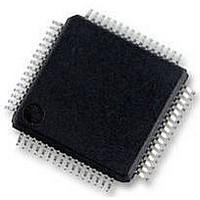
S9S12HY64J0MLH Freescale Semiconductor, S9S12HY64J0MLH Datasheet - Page 141

S9S12HY64J0MLH
Manufacturer Part Number
S9S12HY64J0MLH
Description
MCU 64K FLASH AUTO 64-LQFP
Manufacturer
Freescale Semiconductor
Series
HCS12r
Datasheet
1.S9S12HA32J0CLL.pdf
(792 pages)
Specifications of S9S12HY64J0MLH
Core Processor
HCS12
Core Size
16-Bit
Speed
32MHz
Connectivity
CAN, EBI/EMI, I²C, IrDA, LIN, SCI, SPI
Peripherals
LCD, Motor control PWM, POR, PWM, WDT
Number Of I /o
50
Program Memory Size
64KB (64K x 8)
Program Memory Type
FLASH
Eeprom Size
4K x 8
Ram Size
4K x 8
Voltage - Supply (vcc/vdd)
4.5 V ~ 5.5 V
Data Converters
A/D 6x10b
Oscillator Type
Internal
Operating Temperature
-40°C ~ 125°C
Package / Case
64-LQFP
Controller Family/series
S12
No. Of I/o's
50
Ram Memory Size
4KB
Cpu Speed
64MHz
No. Of Timers
2
Rohs Compliant
Yes
Processor Series
S12HY
Core
HCS12
3rd Party Development Tools
EWHCS12
Development Tools By Supplier
DEMO9S12HY64
Lead Free Status / RoHS Status
Lead free / RoHS Compliant
Available stocks
Company
Part Number
Manufacturer
Quantity
Price
Company:
Part Number:
S9S12HY64J0MLH
Manufacturer:
Freescale Semiconductor
Quantity:
10 000
- Current page: 141 of 792
- Download datasheet (4Mb)
The fixed 16KB page from 0x0000 to 0x3FFF is the page number 0x0C. Parts of this page are covered by
Registers, D-Flash and RAM space. See SoC Guide for details.
The fixed 16KB page from 0x4000–0x7FFF is the page number 0x0D.
The reset value of 0x0E ensures that there is linear Flash space available between addresses 0x0000 and
0xFFFF out of reset.
The fixed 16KB page from 0xC000-0xFFFF is the page number 0x0F.
3.4
The S12PMMC block performs several basic functions of the S12P sub-system operation: MCU operation
modes, priority control, address mapping, select signal generation and access limitations for the system.
Each aspect is described in the following subsections.
3.4.1
3.4.2
3.4.2.1
The BDM firmware lookup tables and BDM register memory locations share addresses with other
modules; however they are not visible in the memory map during user’s code execution. The BDM
memory resources are enabled only during the READ_BD and WRITE_BD access cycles to distinguish
between accesses to the BDM memory area and accesses to the other modules. (Refer to BDM Block
Guide for further details).
When the MCU enters active BDM mode, the BDM firmware lookup tables and the BDM registers
become visible in the local memory map in the range 0xFF00-0xFFFF (global address 0x3_FF00 -
0x3_FFFF) and the CPU begins execution of firmware commands or the BDM begins execution of
hardware commands. The resources which share memory space with the BDM module will not be visible
in the memory map during active BDM mode.
Freescale Semiconductor
PIX[3:0]
•
•
Field
3–0
Normal single chip mode
This is the operation mode for running application codeThere is no external bus in this mode.
Special single chip mode
This mode is generally used for debugging operation, boot-strapping or security related
operations. The active background debug mode is in control of the CPU code execution and the
BDM firmware is waiting for serial commands sent through the BKGD pin.
Functional Description
MCU Operating Modes
Memory Map Scheme
Program Page Index Bits 3–0 — These page index bits are used to select which of the 256 P-Flash or ROM
array pages is to be accessed in the Program Page Window.
CPU and BDM Memory Map Scheme
MC9S12HY/HA-Family Reference Manual, Rev. 1.04
Table 3-6. PPAGE Field Descriptions
Description
S12P Memory Map Control (S12PMMCV1)
141
Related parts for S9S12HY64J0MLH
Image
Part Number
Description
Manufacturer
Datasheet
Request
R
Part Number:
Description:
Manufacturer:
Freescale Semiconductor, Inc
Datasheet:
Part Number:
Description:
Manufacturer:
Freescale Semiconductor, Inc
Datasheet:
Part Number:
Description:
Manufacturer:
Freescale Semiconductor, Inc
Datasheet:
Part Number:
Description:
Manufacturer:
Freescale Semiconductor, Inc
Datasheet:
Part Number:
Description:
Manufacturer:
Freescale Semiconductor, Inc
Datasheet:
Part Number:
Description:
Manufacturer:
Freescale Semiconductor, Inc
Datasheet:
Part Number:
Description:
Manufacturer:
Freescale Semiconductor, Inc
Datasheet:
Part Number:
Description:
Manufacturer:
Freescale Semiconductor, Inc
Datasheet:
Part Number:
Description:
Manufacturer:
Freescale Semiconductor, Inc
Datasheet:
Part Number:
Description:
Manufacturer:
Freescale Semiconductor, Inc
Datasheet:
Part Number:
Description:
Manufacturer:
Freescale Semiconductor, Inc
Datasheet:
Part Number:
Description:
Manufacturer:
Freescale Semiconductor, Inc
Datasheet:
Part Number:
Description:
Manufacturer:
Freescale Semiconductor, Inc
Datasheet:
Part Number:
Description:
Manufacturer:
Freescale Semiconductor, Inc
Datasheet:
Part Number:
Description:
Manufacturer:
Freescale Semiconductor, Inc
Datasheet:


