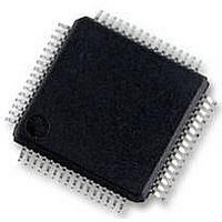
S9S12HY64J0MLH Freescale Semiconductor, S9S12HY64J0MLH Datasheet - Page 477

S9S12HY64J0MLH
Manufacturer Part Number
S9S12HY64J0MLH
Description
MCU 64K FLASH AUTO 64-LQFP
Manufacturer
Freescale Semiconductor
Series
HCS12r
Datasheet
1.S9S12HA32J0CLL.pdf
(792 pages)
Specifications of S9S12HY64J0MLH
Core Processor
HCS12
Core Size
16-Bit
Speed
32MHz
Connectivity
CAN, EBI/EMI, I²C, IrDA, LIN, SCI, SPI
Peripherals
LCD, Motor control PWM, POR, PWM, WDT
Number Of I /o
50
Program Memory Size
64KB (64K x 8)
Program Memory Type
FLASH
Eeprom Size
4K x 8
Ram Size
4K x 8
Voltage - Supply (vcc/vdd)
4.5 V ~ 5.5 V
Data Converters
A/D 6x10b
Oscillator Type
Internal
Operating Temperature
-40°C ~ 125°C
Package / Case
64-LQFP
Controller Family/series
S12
No. Of I/o's
50
Ram Memory Size
4KB
Cpu Speed
64MHz
No. Of Timers
2
Rohs Compliant
Yes
Processor Series
S12HY
Core
HCS12
3rd Party Development Tools
EWHCS12
Development Tools By Supplier
DEMO9S12HY64
Lead Free Status / RoHS Status
Lead free / RoHS Compliant
Available stocks
Company
Part Number
Manufacturer
Quantity
Price
Company:
Part Number:
S9S12HY64J0MLH
Manufacturer:
Freescale Semiconductor
Quantity:
10 000
- Current page: 477 of 792
- Download datasheet (4Mb)
In slave mode, if the SS line is not deasserted between the successive transmissions then the content of the
SPI data register is not transmitted; instead the last received data is transmitted. If the SS line is deasserted
for at least minimum idle time (half SCK cycle) between successive transmissions, then the content of the
SPI data register is transmitted.
In master mode, with slave select output enabled the SS line is always deasserted and reasserted between
successive transfers for at least minimum idle time.
13.4.3.3
Some peripherals require the first SCK edge before the first data bit becomes available at the data out pin,
the second edge clocks data into the system. In this format, the first SCK edge is issued by setting the
CPHA bit at the beginning of the n
The first edge of SCK occurs immediately after the half SCK clock cycle synchronization delay. This first
edge commands the slave to transfer its first data bit to the serial data input pin of the master.
A half SCK cycle later, the second edge appears on the SCK pin. This is the latching edge for both the
master and slave.
1. n depends on the selected transfer width, please refer to
Freescale Semiconductor
End of Idle State
SCK Edge Number
SCK (CPOL = 0)
SCK (CPOL = 1)
SAMPLE I
MOSI/MISO
CHANGE O
CHANGE O
SEL SS (O)
Master only
SEL SS (I)
t
t
t
t
Figure 13-13. SPI Clock Format 0 (CPHA = 0), with 16-Bit Transfer Width selected (XFRW = 1)
MOSI pin
MISO pin
L
T
I
L
MSB first (LSBFE = 0)
LSB first (LSBFE = 1)
, t
= Minimum idling time between transfers (minimum SS high time)
= Minimum leading time before the first SCK edge
= Minimum trailing time after the last SCK edge
T
, and t
CPHA = 1 Transfer Format
I
are guaranteed for the master mode and required for the slave mode.
MSB
LSB
t
L
1
2
Bit 14
Bit 1
3
MC9S12HY/HA-Family Reference Manual Rev. 1.04
4
Bit 13
Bit 2
5
Begin
6
1
Bit 12
Bit 3
-cycle transfer operation.
7
8
Bit 11
Bit 4
9
10
Bit 10 Bit 9 Bit 8 Bit 7 Bit 6
Bit 5
11
12
Bit 6
13
14
Section 13.3.2.2, “SPI Control Register 2 (SPICR2)
Transfer
Bit 7 Bit 8 Bit 9 Bit 10Bit 11Bit 12Bit 13Bit 14
15
16
17
18
19
20
Bit 5
21
22
Bit 4 Bit 3 Bit 2 Bit 1
23
24
25
End
26
27
Serial Peripheral Interface (S12SPIV5)
28
29
30
MSB
LSB
31
32
t
T
Minimum 1/2 SCK
for t
Begin of Idle State
t
I
t
T
L
, t
l
, t
L
477
Related parts for S9S12HY64J0MLH
Image
Part Number
Description
Manufacturer
Datasheet
Request
R
Part Number:
Description:
Manufacturer:
Freescale Semiconductor, Inc
Datasheet:
Part Number:
Description:
Manufacturer:
Freescale Semiconductor, Inc
Datasheet:
Part Number:
Description:
Manufacturer:
Freescale Semiconductor, Inc
Datasheet:
Part Number:
Description:
Manufacturer:
Freescale Semiconductor, Inc
Datasheet:
Part Number:
Description:
Manufacturer:
Freescale Semiconductor, Inc
Datasheet:
Part Number:
Description:
Manufacturer:
Freescale Semiconductor, Inc
Datasheet:
Part Number:
Description:
Manufacturer:
Freescale Semiconductor, Inc
Datasheet:
Part Number:
Description:
Manufacturer:
Freescale Semiconductor, Inc
Datasheet:
Part Number:
Description:
Manufacturer:
Freescale Semiconductor, Inc
Datasheet:
Part Number:
Description:
Manufacturer:
Freescale Semiconductor, Inc
Datasheet:
Part Number:
Description:
Manufacturer:
Freescale Semiconductor, Inc
Datasheet:
Part Number:
Description:
Manufacturer:
Freescale Semiconductor, Inc
Datasheet:
Part Number:
Description:
Manufacturer:
Freescale Semiconductor, Inc
Datasheet:
Part Number:
Description:
Manufacturer:
Freescale Semiconductor, Inc
Datasheet:
Part Number:
Description:
Manufacturer:
Freescale Semiconductor, Inc
Datasheet:


