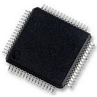
S9S12HY64J0MLH Freescale Semiconductor, S9S12HY64J0MLH Datasheet - Page 71

S9S12HY64J0MLH
Manufacturer Part Number
S9S12HY64J0MLH
Description
MCU 64K FLASH AUTO 64-LQFP
Manufacturer
Freescale Semiconductor
Series
HCS12r
Datasheet
1.S9S12HA32J0CLL.pdf
(792 pages)
Specifications of S9S12HY64J0MLH
Core Processor
HCS12
Core Size
16-Bit
Speed
32MHz
Connectivity
CAN, EBI/EMI, I²C, IrDA, LIN, SCI, SPI
Peripherals
LCD, Motor control PWM, POR, PWM, WDT
Number Of I /o
50
Program Memory Size
64KB (64K x 8)
Program Memory Type
FLASH
Eeprom Size
4K x 8
Ram Size
4K x 8
Voltage - Supply (vcc/vdd)
4.5 V ~ 5.5 V
Data Converters
A/D 6x10b
Oscillator Type
Internal
Operating Temperature
-40°C ~ 125°C
Package / Case
64-LQFP
Controller Family/series
S12
No. Of I/o's
50
Ram Memory Size
4KB
Cpu Speed
64MHz
No. Of Timers
2
Rohs Compliant
Yes
Processor Series
S12HY
Core
HCS12
3rd Party Development Tools
EWHCS12
Development Tools By Supplier
DEMO9S12HY64
Lead Free Status / RoHS Status
Lead free / RoHS Compliant
Available stocks
Company
Part Number
Manufacturer
Quantity
Price
Company:
Part Number:
S9S12HY64J0MLH
Manufacturer:
Freescale Semiconductor
Quantity:
10 000
- Current page: 71 of 792
- Download datasheet (4Mb)
1
2.3.3
Freescale Semiconductor
Function
Address 0x0000 (PRR)
Read: Anytime. The data source is depending on the data direction value.
Write: Anytime
Altern.
Field
7-4,2
Reset
PA
PA
PA
PA
3
1
0
W
R
Port A general purpose input/output data—Data Register, LCD segment driver output
The associated pin can be used as general purpose I/O when not used as alternative function is not enabled. In
general purpose output mode the register bit value is driven to the pin. If the associated data direction bit is set to 1,
a read returns the value of the port register bit, otherwise the buffered pin input state is read.
Port A general purpose input/output data—Data Register, LCD segment driver output, API_EXTCLK
The associated pin can be used as general purpose I/O when not used as alternative function. In general purpose
output mode the register bit value is driven to the pin. If the associated data direction bit is set to 1, a read returns
the value of the port register bit, otherwise the buffered pin input state is read.
Port A general purpose input/output data—Data Register, LCD segment driver output, XIRQ
The associated pin can be used as general purpose I/O when not used as alternative function. In general purpose
output mode the register bit value is driven to the pin. If the associated data direction bit is set to 1, a read returns
the value of the port register bit, otherwise the buffered pin input state is read.
Port A general purpose input/output data—Data Register, LCD segment driver output, IRQ
The associated pin can be used as general purpose I/O when not used as alternative function. In general purpose
output mode the register bit value is driven to the pin. If the associated data direction bit is set to 1, a read returns
the value of the port register bit, otherwise the buffered pin input state is read.
• The LCD segment driver output takes precedence over the general purpose I/O function if the related LCD
• The LCD segment driver output takes precedence over the API_EXTCLK and general purpose I/O function if the
• The API_EXTCLK takes precedence over the general purpose I/O function if the API_EXTCLK function is enabled
• The LCD segment driver output takes precedence over the XIRQ and general purpose I/O function if the related
• The XIRQ takes precedence over the general purpose I/O function if the XIRQ function is enabled
• The LCD segment driver output takes precedence over the IRQ and general purpose I/O function if the related
• The IRQ takes precedence over the general purpose I/O function if the IRQ function is enabled
FP36
Port A Data Register (PORTA)
PA7
segment is enabled.
related LCD segment is enabled.
LCD segment is enabled.
LCD segment is enabled.
—
0
7
FP35
PA6
—
0
6
MC9S12HY/HA-Family Reference Manual, Rev. 1.04
Table 2-4. PORTA Register Field Descriptions
Figure 2-1. Port A Data Register (PORTA)
FP34
PA5
—
5
0
FP33
PA4
—
0
4
Description
API_EXTCLK
FP32
PA3
0
3
FP31
PA2
—
Port Integration Module (S12HYPIMV1)
0
2
Access: User read/write
XIRQ
FP30
PA1
0
1
FP29
IRQ
PA7
0
0
71
1
Related parts for S9S12HY64J0MLH
Image
Part Number
Description
Manufacturer
Datasheet
Request
R
Part Number:
Description:
Manufacturer:
Freescale Semiconductor, Inc
Datasheet:
Part Number:
Description:
Manufacturer:
Freescale Semiconductor, Inc
Datasheet:
Part Number:
Description:
Manufacturer:
Freescale Semiconductor, Inc
Datasheet:
Part Number:
Description:
Manufacturer:
Freescale Semiconductor, Inc
Datasheet:
Part Number:
Description:
Manufacturer:
Freescale Semiconductor, Inc
Datasheet:
Part Number:
Description:
Manufacturer:
Freescale Semiconductor, Inc
Datasheet:
Part Number:
Description:
Manufacturer:
Freescale Semiconductor, Inc
Datasheet:
Part Number:
Description:
Manufacturer:
Freescale Semiconductor, Inc
Datasheet:
Part Number:
Description:
Manufacturer:
Freescale Semiconductor, Inc
Datasheet:
Part Number:
Description:
Manufacturer:
Freescale Semiconductor, Inc
Datasheet:
Part Number:
Description:
Manufacturer:
Freescale Semiconductor, Inc
Datasheet:
Part Number:
Description:
Manufacturer:
Freescale Semiconductor, Inc
Datasheet:
Part Number:
Description:
Manufacturer:
Freescale Semiconductor, Inc
Datasheet:
Part Number:
Description:
Manufacturer:
Freescale Semiconductor, Inc
Datasheet:
Part Number:
Description:
Manufacturer:
Freescale Semiconductor, Inc
Datasheet:


